General Purpose I/O (GPIO) refers to pins on a chip that can be either input or output, and logic-high (0) or logic-low (1), but have no predefined purpose (as opposed to specialized pins that may implement specific protocols, such as RX/TX pins for a UART). GPIO pins are appropriate for simple input and output devices such as switches, buttons, LEDs, etc.
Often we want to control and observe these pins from our software code (reading input pins and setting output pins). This requires a special piece of hardware called a GPIO Controller that interfaces between the processor bus and the actual pins. This allows the processor to interface with the individual pins by reading and writing to specific addresses that belong to the GPIO Controller (See the Address Map section for details about this).
In your lab, you will write a simple driver for the GPIO Controller, which will abstract away the hardware access and provide simple software functions to read the state of the buttons and switches.
Class Slides
Schematic
The schematic showing how the GPIO pins are connected to the buttons and switches on the printed circuit board (PCB) is shown on Page 22 of the ZYBO reference manual, and included here:
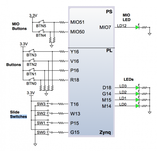
As shown in the schematic, these buttons and slide switches are attached to pins on the Zynq processing chip (mounted on the center of the PCB).
Question: What is the logic value of the pin attached to the push-button when the button is pushed? When it is released?
GPIO Controller
A GPIO controller provides an interface between the processor running software and GPIO pins. On our Zynq processing chip, this hardware is called the AXI GPIO, and is described in this data sheet.
I have included the schematic from page 3 of the data sheet below:
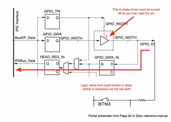
This shows one pin (one bit) of the GPIO connection. The circuit is replicated for each pin of the GPIO controller (so one of these circuits for each slide switch and each push button). There is a separate GPIO controller for the push-buttons and a separate GPIO block for the slide switches. Both GPIO blocks are 4-bits wide because there are 4 push-buttons and 4 slide-switches.
I have annotated the schematic to show the path that the button or slide-switch logic value will take through the GPIO IP. Also, note that each pin of the GPIO block can function as either an input or output. You want all of the GPIO pins to function as an input so you can read the switch and button values. When a pin is functioning as input, the tri-state driver must be turned off; when functioning as an output, the tri-state driver is turned on. You turn the tri-state driver off or on by writing the correct value to the GPIO_TRI register (see Page 9 of the GPIO documentation).
Registers
Each GPIO block provides 4 inputs/outputs so both the GPIO_TRI and GPIO_DATA registers are each 4 bits wide. When reading the GPIO_DATA register, bit 0 corresponds to BTN_0, bit 1 corresponds to BTN_1, etc. When writing the GPIO_TRI register to configure the GPIO so that it provides inputs, bit 0 corresponds to BTN_0, bit 1 corresponds to BTN_1, etc. You will write the GPIO_TRI register in the _init functions so that the GPIO block is setup as having only inputs. See Page 9 of the GPIO documentation for programming details for the GPIO_TRI register.
Even though the hardware registers are only 4 bits wide, when you perform software reads and writes, you will always access them as 32-bit registers, so you can ignore the upper 28 bits of data.
For example, if I read the GPI_DATA register and receive the hexadecimal value 000F (0000_0000_0000_1111 in binary), this means that all push-buttons are depressed. If I read the GPIO_DATA and receive the hexadecimal value 000A (0000_0000_0000_1010), this means that push-buttons BTN_3 and BTN_1 are depressed.
Pro Tip: One way to check to see if hardware is present is to write a write-able register with a value and then read it back to see if the value still exists. If you cannot not successfully write the selected register, the proper hardware may not be present. It would be good to print out an error message in this case to notify the application programmer or user about a catastrophic problem. For example, in the buttons_init() function (for example), you could write the value to the GPIO_TRI register to setup the GPIO hardware to serve as inputs and then read the value back and check to see that it is the correct value.
Accessing Registers from Software
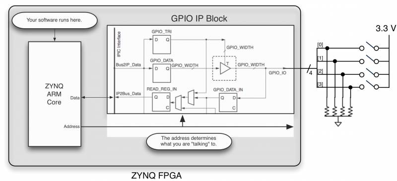
OK, the hardware seems straightforward enough but how do you access the GPIO hardware from software? As you can see in the schematic shown above, three registers are shown (GPIO_TRI, GPIO_DATA, and READ_REG_IN). However, there are only two actual registers that you can access: GPIO_TRI and GPIO_DATA. GPIO_DATA does double duty; when you write it, the value appears at the output (this would be useful for turning on an LED). When you read it, you are reading the value of the switch or button. The Xilinx schematic is a little confusing in this regard. For purposes of this lab, you will only read the GPIO_DATA register. A larger picture that shows how the ARM core, the GPIO block, and the switches are organized is shown below.
The documentation for the AXI GPIO contains a specific section that discusses the registers available to the processor. This critical information is commonly found in datasheets for hardware devices, and provides you with the information you need to interface between software and hardware, and write a device driver. A summarizing table from this section is included here:
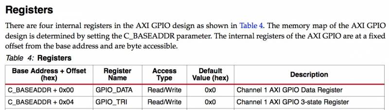
The table shows the addresses in the Address Map that correspond to each registers. However, because the Zynq processing chip we are using is a reconfigurable device (FPGA), the addresses are not fixed and can be chosen by the user when the system is designed. As such, the addresses are not listed as absolute addresses, but rather as offsets from a chosen base address.
So for example, if the base address was 0x12340000, then the GPIO_DATA register would be located at address 0x12340000 and the GPIO_TRI register would be at address 0x12340004.
Base Addresses
The configured base addresses for our system can be found in xparameters.h. This file contains some content similar to this:
/* Definitions for peripheral GPIO_PUSH_BUTTONS */
#define XPAR_PUSH_BUTTONS_BASEADDR 0x41240000
#define XPAR_PUSH_BUTTONS_HIGHADDR 0x4124FFFF
#define XPAR_PUSH_BUTTONS_DEVICE_ID 3
#define XPAR_PUSH_BUTTONS_INTERRUPT_PRESENT 1
#define XPAR_PUSH_BUTTONS_IS_DUAL 0


/* Definitions for peripheral GPIO_SLIDE_SWITCHES */
#define XPAR_SLIDE_SWITCHES_BASEADDR 0x41280000
#define XPAR_SLIDE_SWITCHES_HIGHADDR 0x4128FFFF
#define XPAR_SLIDE_SWITCHES_DEVICE_ID 4
#define XPAR_SLIDE_SWITCHES_INTERRUPT_PRESENT 1
#define XPAR_SLIDE_SWITCHES_IS_DUAL 0
Please note that this excerpt is only an example of what the xparameters.h file could contain. You should never hardcode these values in your program. Always #include "xparameters.h" in your code and use the constants defined there.
For this lab, you only need to know the base address for the push buttons (XPAR_PUSH_BUTTONS_BASEADDR) and the slide switches (XPAR_SLIDE_SWITCHES_BASEADDR). You can ignore all of the other lines with #define.
Accessing Device Registers
Armed with a knowledge of the base addresses for the two GPIO blocks, how do you access GPIO registers via ‘C’? Xilinx makes it very simple. There are two functions defined in “xil_io.h” that you should use:
uint32_t Xil_In32(uint32_t Addr); // Returns the value at the address.

void Xil_Out32(uint32_t Addr, uint32_t Value);  // Writes value to the address.
Before using these functions you should #include "xil_io.h" at the top of your program. You can find xil_io.h at zybo/xil_arm_toolchain/bsp/ps7_cortexa9_0/include/xil_io.h.
Helper functions
Rather than calling these register access functions throughout your driver code, you should instead create helper functions. Here is an example of helper functions to use for the buttons driver:
static uint32_t readRegister(uint32_t offset) {
   return Xil_In32(XPAR_PUSH_BUTTONS_BASEADDR + offset);
}

static void writeRegister(uint32_t offset, uint32_t value) {
   Xil_Out32(XPAR_PUSH_BUTTONS_BASEADDR + offset, value);
}
While it may seem silly to create extra functions that are so simple, it is a good design practice to abstract away the hardware access functions. As you write more complex drivers that have many accesses to registers, the simpler helper functions will make your code cleaner, more readable, and less likely to contain mistakes and bugs.