Table of Contents
Overview
In an effort to create a standardized way to access the internals of increasingly small circuits for testing and manufacturing, the Joint Test Action Group created the industry standard JTAG. This standard became official in 1990. Testing PCB’s from the outside was becoming infeasible, and so JTAG provides a standardized way to see what is going on in a circuit without having to use big traditional electronic tools.
Some Vocabulary:
JTAG is the interface
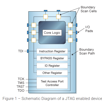
Boundary Scan is the test tech where cells are placed on I/O pins
1149.1 is the standard
“The IEEE standard defines the Test Access Port (TAP), a sequential state machine called the TAP controller that’s implemented in the IC, the Instruction Register, and a number of Data Registers.” See more here
We use JTAG in the Configurable Computing Lab to effectively read status registers and configure, among other things.
Test Access Port (TAP)
TAP (Test Access Port) includes the following connections (these descriptions are from the persepctive of the JCM):
- TCK (Test Clock): Outbound clock signal
- TMS (Test Mode Select): Outbound signal that controls the state machine
- TDI (Test Data In): Outbound signal that shifts data out (sampled on the falling edge of TCK)
- TDO (Test Data Out): Inbound signal that shifts data in (sampled on the rising edge of TCK)
- TRST (Test Reset OPTIONAL): Sends state machine to Reset state
ACTIVITY
▼
Fill in the blank
TAP stands for ___.
ACTIVITY
▼
Match each signal with its function.
- TDO
- TMS
- TDI
- TCK
- Output from JTAG enabled device
- Change state for TAP controller
- Input from JCM
- Clock signal
TAP Controller
Here is a helpful animation to understand the state machine, the registers, and the modes. You can find a static diagram here.
The JTAG Protocol shifts data out and in together, right after each other. For example if we wanted to input 0x9 via TDI, we would get output via TDO:
| Clock | Device | Output | Input |
|---|---|---|---|
| 0 | 0110 | 0 | 1 |
| 1 | 1011 | 1 | 0 |
| 2 | 0101 | 1 | 0 |
| 3 | 0010 | 0 | 1 |
| 4 | 1001 |
This shifting occurs in designated shift registers. This makes it necessary to include two additional steps in reading and writing data, capture and update. Capture loads values from a source register into a shift register. Update loads values from the shift register back into the source register. This ensures that you don’t accidentally start using half-inputted values.
States
- Test Logic Reset: Initial state. Sending
0b11111will always result in the state machine returning to Test Logic Reset, no matter what state it started in. - Run Test Idle: Idle state that the state machine remains in until TMS goes high.
- Select DR Scan: Beginning of the Data Register path. State allows us to choose whether to work on the Data Register or work on the Instruction Register.
- Capture DR: Loads the information from the register signalled by the Instruction Register into the Data Shift Register. Essentially takes a snapshot of the data we want to look at and puts it into a register that we can shift it out from.
- Shift DR: Each time a new bit gets fed into TMS, the Shift DR state shifts a bit out via TDO and shifts a bit in via TDI. To shift 4 bits into the Data Shift Register, TMS would need to be 0001, as a bit gets shifted when Shift DR transitions to Exit 1 DR.
- Exit 1 DR: Exits to either the Pause DR state or the Update DR state. If the main device is done shifting in data, then we can move on to Update DR. If the main device is not done shifting in data, then we can move to Pause DR.
- Pause DR: Lets the JTAG enabled device wait if it needs to without updating the register signalled by the Instruction Register. (usually only done if the main device needs time to prepare data to send)
- Exit 2 DR: Exits to either Shift DR (shift more data) or Update DR (we’re done shifting data).
- Update DR: Loads the (newly shifted in) information from the Data Shift Register back into the register signalled by the Instruction Register.
- Select IR Scan: State allows us to return to Test Logic Reset or continue on to working on the Instruction Register.
- Capture IR: Loads status information into the Instruction Shift Register. Since we are shifting data, this allows us to easily check the connection and status.
- Shift IR: Each time a new bit gets fed into TMS, the Shift IR state shifts a bit out via TDO and shifts a bit in via TDI.
- Exit 1 IR: Exits to either the Pauase IR state or the Update IR state. If the main device is done shifting in data, then we can move on to Update IR. If the main device is not done shifting in data, then we can move to Pause IR.
- Pause IR: Lets the JTAG enabled device wait if it needs to without updating the Instruction Register. (usually only done if the main device needs time to prepare data to send)
- Exit 2 IR: Exits to either Shift IR (shift more data) or Update IR (we’re done shifting data).
- Update IR: Loads the (newly shifted in) information from the Instruction Shift Register into the Instruction Register.
ACTIVITY
▼
Fill in the blank
What bits do you send to return the TAP controller to Test Logic Reset? ___
ACTIVITY
▼
When does the value of TDI matter?
- Capture DR
- Shift IR
- Select DR Scan
- Run Test Idle
You may notice that the state machine always follows the order of capture, shift, and update. There is no way to bypass these options. To the JTAG enabled device, reading and writing always happen together (unless the memory is read-only, in which case writing is ignored automatically). For writable memory, in order to avoid overwriting data when you just want to read it, TDI and TDO run on different edges of the clock cycle. This enables the JCM (main device) to read the output from the JTAG enabled device and then use that as an input, writing the exact same data that was already there.
Instruction Register (IR)
The Instruction Register contains the information as to which Data Register the Data Shift Register should pull information from and send information back to.
Common sizes for an Instruction Register include 4, 6, and 8 bits. You’ll probably notice that this is nowhere near large enough to address the vast majority of the JTAG-enabled device. In order to get data from anywhere other than the few registers that the Instruction Register accesses directly, you need to use a larger Data Register to store the address.
Since JTAG works by shifting data, do you think that a single main device can communicate through JTAG with devices daisy-chained together. The main device just has to know how large the Instruction Register is for each device so that it can know how far it needs to shift bits.
Data Registers (DR)
JTAG-enabled devices have different Data Registers for different purposes.
One of the data registers is the BYPASS register. This improves efficiency when multiple devices are communicating through JTAG with a main device. The BYPASS register is only one bit. It is addressed to when the IR is all 1’s.
Another is the IDCODE register. Gives you the ID code, which allows you to identify the chip. This is read-only memory, so it doesn’t get overwritten.
Activities
Set to BYPASS
Write out the bitstreams for TMS and TDI to set a device’s Data Register to the BYPASS register and then return to Test Logic Reset. Test your answer by referring to the TAP controller state machine.
Learn More
Helpful links:
- Overview
- State Machine and Pictures (SM and JTAG pics)
- High level guide
- JTAG Tutorial