Table of Contents
In this lab you will create a hardware system of your choice on the FPGA, and then insert a temperature-controlled Trojan into the system.
Preliminary
Trojan Taxonomy
The taxonomy of Trojan circuits has been presented in various forms, and it continues to evolve as newer attacks and Trojan types are discovered. The figure below shows a high-level classification based on variations in activation mechanism and Trojan effect.
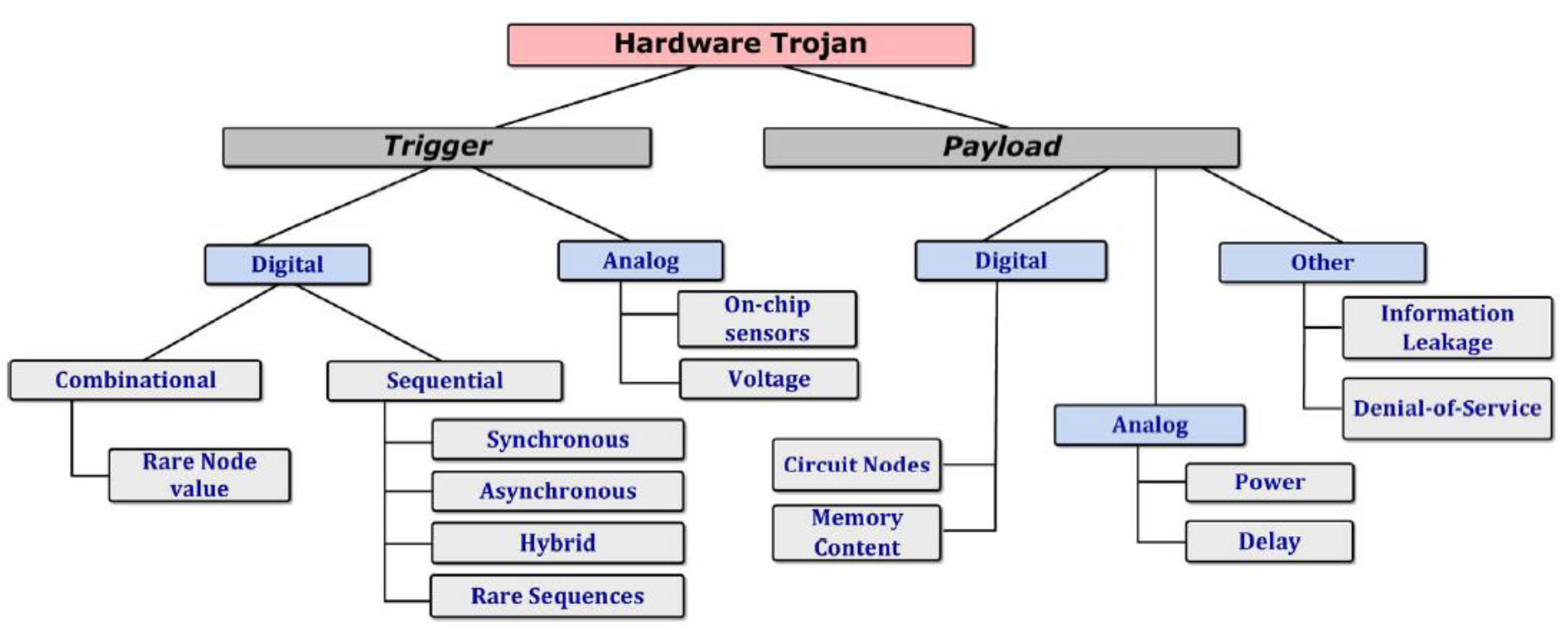
Based on the trigger condition, the hardware Trojans can be classified into analog or digital Trojans. The former is activated by analog conditions such as temperature, delay, or device aging effect, whereas the latter are triggered by some Boolean logic function. Digitally triggered Trojans can again be classified into combinational and sequential types.
In terms of the payload, the Trojan can cause functional failure upon triggering or have a passive effect such as heating of the die or leaking of information. A Trojan can cause an ‘‘information leakage’’ attack, where secret information is leaked by a Trojan via a transmitted radio signal or serial data port. It could also involve a side-channel attack where the information is leaked through the power trace or through thermal radiation or through optical modulation of an output LED. Another type of Trojan payload would be an unauthorized alteration in system behavior.
Hard-to-Detect Circuit Behaviors
Recently Intel announced a flaw in the implementation of the “TSX” instruction for its Haswell series of Central Processing Unit (CPU). This announcement came almost a year into the product’s lifecycle and almost three years since the beginnings of Haswell’s architecture was laid out. This is a legitimate mistake on Intel’s part – there is no foul play or trickery here, although it shows how difficult it is to fully test a complex design.
Researchers at the University of Massachusetts were able to modify an Intel Ivy Bridge processor – the series that Haswell replaced – and significantly impair the Random Number Generator (RNG) of the processor. They did this by modifying the silicon that made up actual transistor. Their modification is completely undetectable without a Scanning Electron Microscope (SEM) and a known good chip to authenticate against. If the security of the RNG is compromised then everything generated from it is also compromised, for example, private encryption keys.
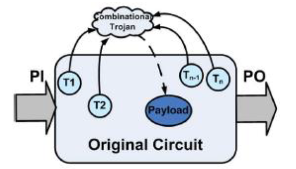
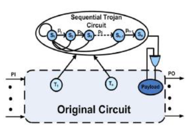
An intelligent adversary is expected to hide such tampering with an IC’s behavior in a way that makes it extremely difficult to detect with conventional post-manufacturing testing. Intuitively, it means that the adversary would ensure that such tampering is manifested or triggered under very rare conditions at the internal nodes, which are unlikely to arise during testing but can occur during long hours of field operation.
The figures below show general models of combinational and sequential Trojans. These abstract models of Trojans are useful for studying the space of possible Trojans, and, similar to fault models, help in test vector generation for Trojan detection.
DES
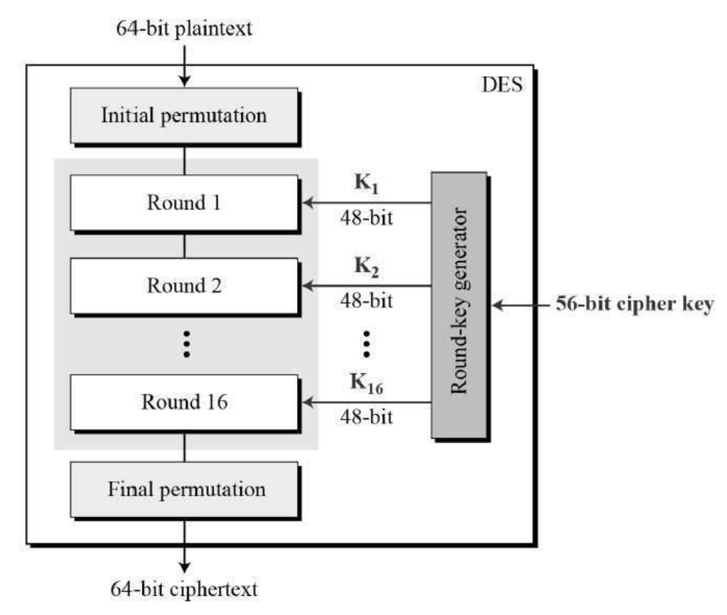
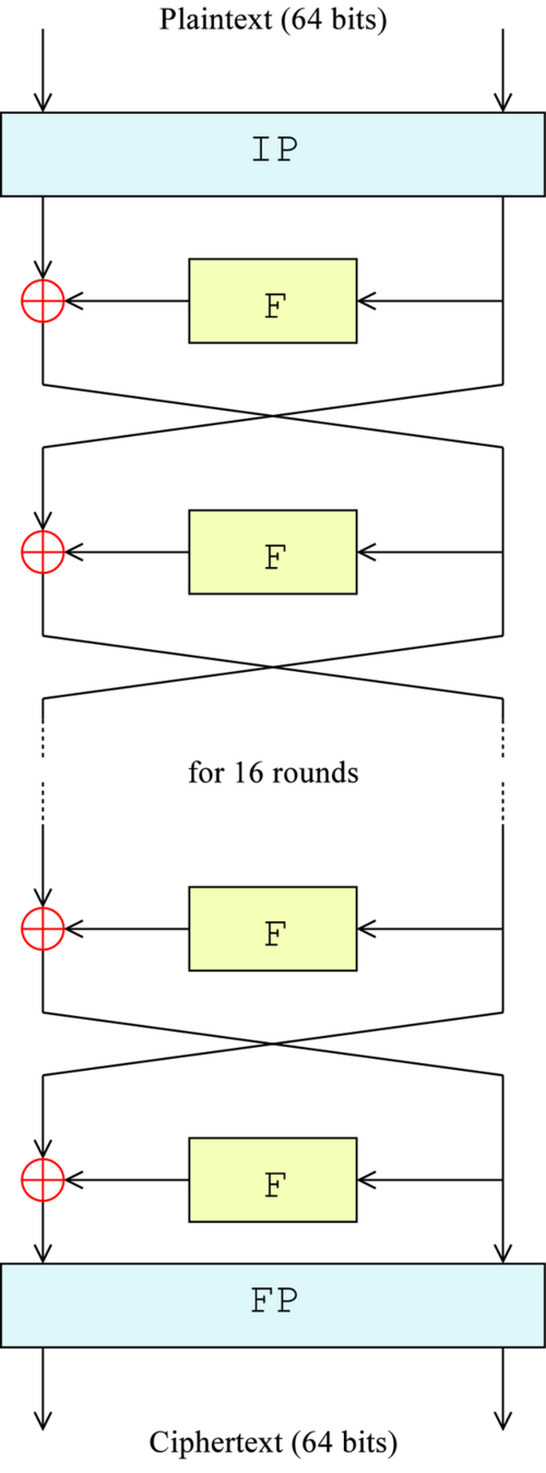
DES is a symmetric-key algorithm for encrypting electronic data. Although it is now considered insecure, it was highly influential in the advancement of modern cryptography. It uses 16 round Feistel structure. The block size is 64-bit, of which DES has an effective key length of 56 bits, since 8 of the 64 bits of the key are parity bits used for error correction and are not used by the encryption algorithm. The encryption steps are illustrated in the figure below.
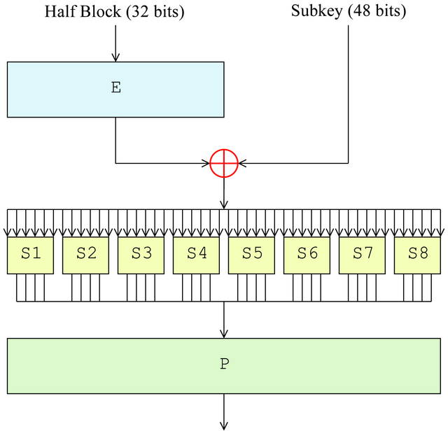
The left image below shows how data is processed in each round, and the right image shows the Feistel function (F-function) used in each round.
More details about DES can be found here.
Lab Directory
You will be using the lab_trojan_i directory for this lab.
You have been provided several 12 Verilog files related to the DES implementation on the FPGA.
Instructions
Part I: Implement DES
- Create a subdirectory in your folder, called
part1. - Within this, create a new GOWIN project called
part1with top module calledtop, that instantiates thedesmodule fromdes.vfile. See the Creating Projects section on the GOWIN Tutorial page for instructions on creating a new project.- There are two modules inside this file:
desanddes_o. des_ocontains the DES implementation, anddesis the wrapper top module that instantiatesdes_o.- Plaintext and key are given in
des. - There is a RAM module called
ram1instantiated, which is a 64-bit wide, 32-word deep RAM. It will store all the encryption results of the 16 rounds. - Refer to the appendix for starting this project.
- There are two modules inside this file:
- Compile and program the FPGA.
- Use the Gowin Analyzer Oscilloscope (GAO) to view the DES encryption.
- The encryption process happens repeatedly, so you can use GAO to view the signals repeatedly performing the encryption; however, after the first encryption cycle (which happens very fast, before you can start capture with GAO), the result in the RAM should not change.
- If you look at
des.v, you will see the clock is being slowed down by 50x, resulting in a 1MHz clock. You may want to clock the logic analyzer using this slower clock signal so that you are not viewing the same data repeatedly. You can shorten the capture window down to 32, which will be large enough to capture all rounds of encryption at least once.
- REPORT: Answer the following questions in your report:
-
Use the plaintext and key provided and add them in the `des.v Verilog file:
desIn = 64'hA42F891BD376CE05
key64 = 64'h0123456789ABCDEF
Store all the encryption results for the 16 rounds in an implemented RAM and show the result of the final round (upper 64 bits of the 1024-bit RAM). You can verify the correct encryption using an online tool, such as http://des.online-domain-tools.com/
- Which module is creating the key for each round? How?
- Which module is doing the Feistel function?
- How many Logic Elements are used?
-
Part II: Insert a combinational Trojan
- Create a new folder,
part2, that contains a new Gowin project. Start with a working DES circuit, identical to what you did in Part 1 (You can copy all of the files into thesrcdirectory for this new project). - Insert a combinational Trojan into the DES circuit.
- The trigger condition of the Trojan is when the output of the F function (Figure 6) satisfies for some value of the least significant 4 bits (see next section).
- When the Trojan is triggered, the LSB of the input key (NOT round keys) for the DES is inverted (ie. invert key56[0]).
- When the trigger condition is not true, the key becomes the original input key.
- You will want to register your trigger signal to prevent a combinational loop from occurring. That means that in any cycle where the trigger is true, the following cycle will have key56[0] inverted.
- REPORT: Answer the following questions in your report:
- When the trigger condition is 4’b0110, will the Trojan be triggered? How many times is it triggered in the 16 rounds? Turn in a screenshot of the GAO window.
- When the condition is 4’b1001, repeat answering question 1. again. Take another screenshot of the GAO window.
- When the condition is 4’b1010, repeat answering question 1. again. Take another screenshot of the GAO window.
Part III: Insert a sequential Trojan
- Create a new folder,
part3, that contains another new Gowin project. Once again, copy over your working DES design from Part 1. - Insert a sequential Trojan into the DES circuit.
- Use the same clock as the DES circuit.
- The trigger condition of the Trojan is when the least significant 2 bits of the F function output in order go through some order of three values in consecutive clock cycles.
- Like Part II, when the Trojan is triggered, the LSB of the input key (NOT round keys) for the DES is inverted (ie. invert key56[0]). The key only needs to be inverted for one cycle, and can then revert to the original value.
- REPORT: Answer the following questions in your report:
- Consider the sequential trigger
2'b01→2'b11→2'b01a. How many states are needed in total? b. How many additional registers are required in the FPGA? c. Will the Trojan be triggered? Turn in a screenshot of the GAO window. - When the condition is
2'b01→2'b11→2'b10, will the Trojan be triggered? Turn in a screenshot of the GAO window. You can just modify your trojan to detect this pattern instead of the previous one (you don’t need a trojan that detects both patterns). - Find another sequence of three 2-bit values that will trigger the Trojan. What is the sequence? Turn in a screenshot of the GAO window.
- Consider the sequential trigger
What to Submit
Make sure to tag your submission as lab_trojan_i on Github, and make sure it includes the following files:
- Your lab report (
lab_trojan_i/report.pdf). - The files for all three of your FPGA projects (
lab_trojan_i/part1/,lab_trojan_i/part2/, andlab_trojan_i/part3/). Make sure these contain your verilog source files (with changes to implement the Trojans), as well as your GAO files you used to test the Trojans.
Acknowledgement
These instructions were originally from Dr. Swarup Bhunia, University of Florida, and were modified for this class.
Helpful Tips
Verilog Bit Ordering (MSB/LSB)
When working with Verilog, it’s important to understand how bit ordering works, especially when defining vectors (buses) and referencing the most significant bit (MSB) and least significant bit (LSB).
- Vector Declaration:
[31:0]means the vector has 32 bits, with bit 31 as the MSB and bit 0 as the LSB. The left number is the MSB, and the right is the LSB.[0:31]is also a 32-bit vector, but now bit 0 is the MSB and bit 31 is the LSB. This is less common, but legal in Verilog.[1:32]is also a 32-bit vector, with bit 1 as the MSB and bit 32 as the LSB. This is also legal but less common.