Table of Contents
In this lab you will implement a Simple Power Analysis (SPA) side channel attack on a modular exponentiation circuit.
Preliminary
Background
In cryptography, a side channel attack is any attack based on information gained from the physical implementation of a cryptosystem, rather than brute force or theoretical weaknesses in the algorithms (compare cryptanalysis). For example, timing information, power consumption, electromagnetic leaks or even sound can provide an extra source of information, which can be exploited to break the system. Some side-channel attacks require technical knowledge of the internal operation of the system on which the cryptography is implemented, although others such as differential power analysis are effective as black-box attacks. Many powerful side-channel attacks are based on statistical methods pioneered by Paul Kocher.
When analyzing the security of a cryptographic hardware module, it can be useful to perform a systematic review of the attack surface — the set of physical, electrical and logical interfaces that are exposed to a potential opponent. According to this observation, side channel attacks can be divided into the following classes: invasive attacks, semi-invasive attacks, and non-invasive attacks.
- An invasive attack involves de-packaging to get direct access to the internal components of cryptographic modules or devices. A typical example of this is that the attackers may open a hole in the passivation layer of a cryptographic module and place a probing needle on a data bus to see the data transfer.
- The concept of semi-invasive attack is first developed by Skorobogatov and Anderson. This kind of attack involves access to the device, but without damaging the passivation layer or making electrical contact other than with the authorized surface. For example, in a fault-induced attack, the attacker may use a laser beam to ionize a device to change some of its memories and thus change the output of this device.
- A non-invasive attack involves close observation or manipulation of the device’s operation. This attack only exploits externally available information that is often unintentionally leaked. A typical example of such an attack is timing analysis: measuring the time consumed by a device to execute an operation and correlating this with the computation performed by the device in order to deduce the value of the secret keys.
In this experiment, we will focus on power attacks. Power attacks measure the circuit’s processing time and current consumption to infer what is going on inside it. Of all types of SCA attacks known today, the number of literature on power analysis attacks and the relevant countermeasures is the biggest. Power analysis attack is the current research focus of side-channel attacks. Power analysis attacks have been demonstrated to be very powerful attacks for most straightforward implementations of symmetric and public key ciphers.
Basically, power analysis attack can be divided into SPA and DPA. In SPA attacks, the aim is essential to guess from the power trace which particular instruction is being executed at a certain time and what values the input and output have. Therefore, the adversary needs an exact knowledge of the implementation to mount such an attack. On the other hand, DPA attack does not need the knowledge of the implementation details and alternatively exploiting statistical methods in the analysis process. DPA is one of the most powerful SCA attacks, yet it can be mounted using very little resources.
In this lab you will perform an SPA attack, and in the following lab you will perform a DPA attack.
Modular Exponentiation
You will implement a SPA on square and multiply algorithm, which is often used to implement modular exponentiation functions. The algorithm to calculate xe mod 𝑁, is shown below.
SquareMult(x, e, N):
    let e[n], ..., e[1] be the bits of e
    y = 1
    for i = n downto 1 do
        y = y * y
        y = y mod N
        if e[i] == 1 then
            y = y * x
            y = y mod N
    return y
We can see that there is an if-statement controlled by the value of e. If e[i] (ith bit of e) is zero, only two steps will be needed: square and modulus. Otherwise, if e[i] is one, four steps will be needed: square, modulus, multiply, and another modulus. Therefore, in the case when e[i] is one, the algorithm tends to consume more power (or time, in some cases). We can implement the algorithm into the FPGA and measure how much power it consumes.
Provided Hardware Impelementation
The code for square and multiply algorithm is provided to you. mul.v is the top module, and other.v contains all the submodules.
Instructions
Part 1: Synthesize and Implement the Design
Create a top module that connects mul to the board I/O.
- Make sure to connect the output to an I/O (eg. LEDs), otherwise the circuit will be optimized away.
- A synthesis constraints file is included (synth_constraints.gsc), which will ensure the tool uses the FPGA fabric instead of DSPs to implement the circuit. Make sure and include this in your project. The FPGA does not have enough DSPs to implement this circuit, so you will get an error if you do no include it.
- After synthesizing, check the Hierarchy tab to make sure it wasn’t optimized away. The mul module should require about 1500 LUTs and 2900 ALUs.
Part 2: Capture Power Traces
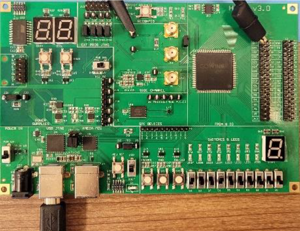
You can find R17, which is a very precise small resistor on the board. This is known as a shunt resistor. The current consumed by the core of the FPGA will all go through this resistor. Therefore, the more power the FPGA consumes, the voltage drop across the resistor will be bigger.
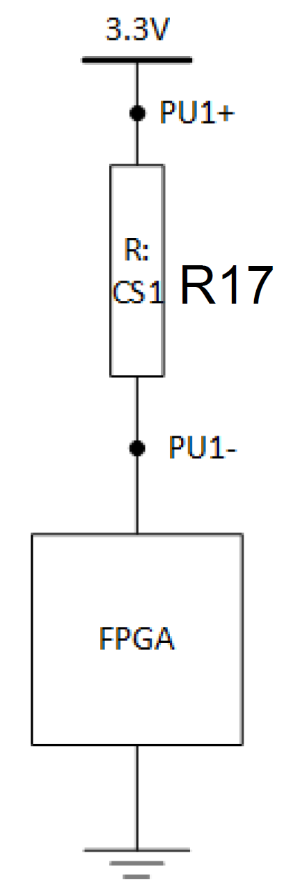
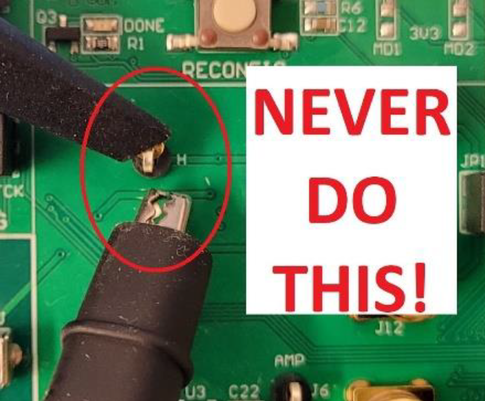
Use the oscilloscope to measure the voltage difference across R17, as shown in the figure below on the left. This measures from the top of R17 to ground. Do not connect the probes directly to the two pins of R17 as shown in the figure on the right below, because the alligator clip of the probe is grounded, which will ground the power delivery to the FPGA. Actually, the picture on the left incorrect as well. It shows probing J8; however, this is the point between the power regulator and the resistor. You actually want to probe J7, which is “after” the resistor (ie. between the resistor and FPGA VCC input). You will also want to remove jumper JP1, which will bypass the resistor. Make sure to put this jump back after completing the lab.
The image below shows an example of the voltage when e=8’b11110000 (this is using a different oscilloscope than what is available in the lab, so the interface may look different).
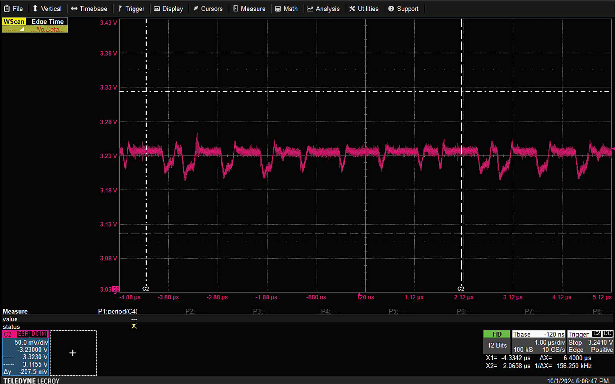
Change the key (value of e) to see how the power consumption changes.
REPORT: Include the following in your lab report and submission:
- The input clock (50 MHz) is slowed down by the
divimodule.- What is the period of the new clock (mul/clk)?
- How many cycles does it take to rotate through the
evalue? Given this, what should be the period of the repeating power usage pattern? Hint: look at the picture above to verify your answer.
- Take a picture of the oscilloscope when
eis8'b01110001. Zoom appropriately to show a full period of the computation.
Part 3: Perform SPA to Recover the Key
- Try the bitstream files
KeyA.fs,KeyB.fs, andKeyC.fs. - REPORT:
- What is the value of
efor each of the bitstream files? (Don’t worry if you guess a “rotated” value of e).
- What is the value of
What to Submit
Tag your submission as lab_spa and make sure to commit your lab report (lab_spa/report.pdf).
Acknowledgement
These instructions were originally from Dr. Swarup Bhunia, University of Florida, and were modified for this class.