Table of Contents
The objective of this experiment is to simulate a Modchip attack towards a system that is protected by a key.
Preliminary
System Overview
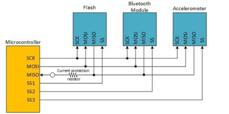
The figure below shows a simplified schematic view of the Microcontroller and flash memory which provides key to the system. Modchipping this FLASH will cause the system to get a different key (usually a more powerful key). In this experiment, we will change the key data that is communicated through the SPI bus without replacing the FLASH memory. We can force the data on the MISO wire to different values by connecting the Modchip soldering point (please find on P2 or P9) to another source. To make things simpler, we’ll short it to ground in this experiment.
About Modchip Attacks
A Modchip is a small electronic device used to alter or disable artificial restrictions of computers or entertainment devices. Modchips are mainly used in video game consoles, DVD players, TV cables, etc. They introduce various modifications to its host system’s function, including the circumvention of region coding, digital rights management, and copy protection checks for the purpose of using media intended for other markets, copied media, or unlicensed third-party software.
Modchips replace or override a system’s hardware or software protection. They achieve this by either exploiting existing interfaces in an unintended or undocumented manner or by actively manipulating the system’s internal communication, sometimes to the point of re-routing it to substitute parts provided by the Modchip.
Most of the Modchips consist of one or more integrated circuits (microcontrollers, FPGAs, or CPLDs), often complemented with discrete parts, usually packaged on a small PCB to fit within the console system it is originally designed for. Although there are Modchips that can be reprogrammed for different purposes, most of the Modchips are designed to work within only one console system or even only one specific hardware version.
Modchips typically require some degree of technical acumen to install since they must be connected to a console’s circuitry, most commonly by soldering wires to select traces or chip legs on a system’s circuit board. Some Modchips allow for installation by directly soldering the Modchip’s contacts to the console’s circuit (“quick solder”), by the precise positioning of electrical contacts (“solderless”). In rare cases, they can be plugged into a system’s internal or external connector.
The diversity of hardware Modchips operates on varying methods. While Modchips are often used for the same goal, they may work in vastly different ways, even if they are intended for use on the same console. Some of the very first Modchips for the Nintendo Wii known as drive chips, modify the behavior and communication of the optical drive to bypass its security. While on the Xbox 360, a common Modchip took advantage of the fact short periods of instability in the CPU could be used to fairly reliably lead it to incorrectly compare security signatures. The precision required in this attack meant the Modchip made use of a CPLD. Other Modchips, such as the XenoGC and clones for the Nintendo GameCube, invoke a debug mode where security measures are reduced or absent, in this case, a stock Atmel AVR microcontroller was used. The most recent innovations are optical disk driven emulators or ODDE, these replace the optical disk drive and allow data to come from another source by bypassing the need to circumvent any security. These often make use of FPGAs to enable them to accurately emulate timing and performance characteristics of the optical drives.
The Test Program
To check for correctness of your Modchip attack, you will use a simple test program, test_program.hex, that will run on the microcontroller. This program will do the following:
- Read the device ID of the flash memory, print it to the UART, and verify it is correct. If it is not correct, the program will halt.
- Wait 1 second.
- Read the 8-bit key from page address
0x0101, column address0x0202of the flash memory, and print it to the UART. - If the key is the USER key (
0x67), the program will print a message indicating it is entering user mode, and repeatedly print-to the UART. - If the key is the ADMIN key (
0x00), the program will print a message indicating it is entering admin mode, and repeatedly print+to the UART. - If the key is the SECRET key (
0xAA), the program will print a message indicating it is entering secret mode, and repeatedly printSto the UART.
Because the program will read the device ID before reading the key, you will need to time your Modchip attack appropriately. If you short the Modchip soldering point to ground too early, the device ID will be incorrect, and the program will halt. If you short it too late, the program will have already read the key, and you will not be able to change it.
Flash Memory
Another objective of this lab is to gain experience interfacing with a SPI flash memory. The flash memory on the board is a Winbond W25N01GV chip. The datasheet for this chip can be found in your docs/ directory here.
Before using the flash memory, you should call haha_spi_init() and haha_flash_init() to initialize the SPI peripheral and pins to the flash memory. Once you have done this, you can communicate with the flash memory using on the SPI bus using the SPI_MasterTransceiveByte(&spiMasterC, <val>) function. This same function can be used for reading and writing to the bus. However, there are multiple devices on the SPI bus, so you will need to activate the chip select (CS) pin for the flash memory before communicating with it, and deactivate it when you are done. For example, to send a byte to the flash memory, you would do the following:
W25N_ss_en();
SPI_MasterTransceiveByte(&spiMasterC, <val>);
W25N_ss_di();
and to get a byte from the flash memory, you would do the following:
W25N_ss_en();
val = SPI_MasterTransceiveByte(&spiMasterC, 0x00); // send dummy data while reading
W25N_ss_di();
You will need to read the datasheet to learn how to communicate with the flash memory. Some things to keep in mind:
- Reading and writing are two-stage processes. For example to read from the flash, you must first move a page from flash memory into an internal buffer, and then read the data from the buffer. Likewise for writing.
- Writing is even more involved, as you must make sure writing is enabled and that write protection is disabled.
- Furthermore NAND flash memory can only be written 1->0, so before writing to a page, you must erase it (set all bits to 1) first.
- Some operations take time to complete, and you must make sure to wait for them to finish before proceeding.
Lab Directory
You will be using the lab_modchip directory for this lab.
Instructions
Step 1: Interacting with the flash Memory
Begin by creating a simple main.c program that will print the device ID of the flash memory to the UART. The documentation shows the correct device ID that will be expected by the test program. Make sure you can get the correct device ID before proceeding.
Step 2: Writing the USER key to the flash memory
Next, extend your program to write the user key (0x67) to page address 0x0101, column address 0x0202 of the flash memory.
After writing the key, read it back and print it to the UART to verify it was written correctly. Make sure you can successfully write and read back the USER key before proceeding. Your main.c program is now complete. Make sure to commit to your repository.
Step 3: Easy Modchip Attack
Enter the ADMIN mode by shorting the appropriate signal to ground.
REPORT: In a single terminal window, run the test program and demonstrate that you can enter USER mode. Then, press the MCU RST key to run the test program again, and use your Modchip attack to enter ADMIN mode. Take a screenshot of the terminal window showing both modes, and include it in your lab report.
Step 4: Hard Modchip Attack (Bonus 10%)
Enter the SECRET mode by connecting a signal generator to the appropriate signal and providing the SECRET key. Be careful to not provide more than 3.3V to the board. Check the signal generator’s output with the oscilloscope before connecting it to the board. This video might help if you are seeing double the voltage you are expecting
REPORT: Take a photo of your setup showing the signal generator connected to the board, and include it in your lab report. Include a screenshot of the terminal window showing that you have successfully entered SECRET mode in your lab report. Describe what signal you connected the signal generator to, and what settings you used on the signal generator (waveform type, frequency, amplitude, offset, etc).
What to Submit
Commit your main.c and create a lab report document that contains the items mentioned above. Make sure to save this as lab_modchip/report.pdf,
and submit as tag lab_modchip, using the submission instructions.
Acknowledgement
These instructions were originally from Dr. Swarup Bhunia, University of Florida, and were modified for this class.