Table of Contents
Creating Projects
The following are the steps to create a project on the GOWIN FPGA Designer software
-
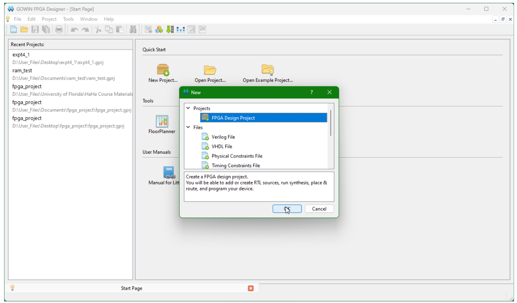
Go to File > New, and select FPGA Design Project.
-
Type the name of the project and its location. Click Next.
For example, for Part 1 of the Trojan I lab, create a directory called
part1inside thelab_trojan_idirectory, and name the projectpart1. -
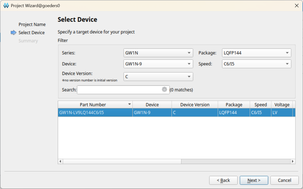
Select the device according to the screenshot below. Click Next and then Finish.
-
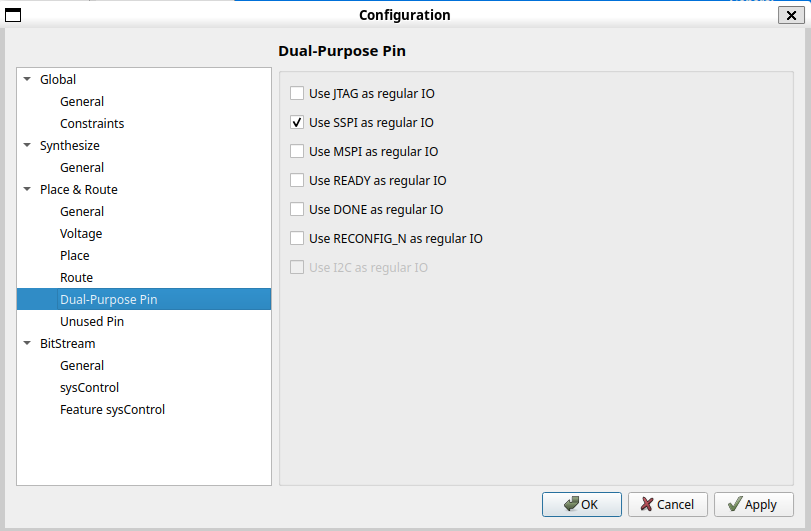
Open the Project->Configuration window, go to Place & Route->Dual-Purpose Pin, and check Use SSPI as regular IO.
-
Copy any files needed to your
srcdirectory.For example, for Part 1 of the Trojan I lab, copy all of the provided Verilog files into the
srcdirectory of your project. -
Copy the provided
gowin_pin_assignments.cstto thesrcdirectory. -
In the GOWIN FPGA Designer window, add existing files by right clicking on the left sidebar. Click Add Files… button. Select all the files inside src directory (including all
.vfiles and the.cstfile). Click Open.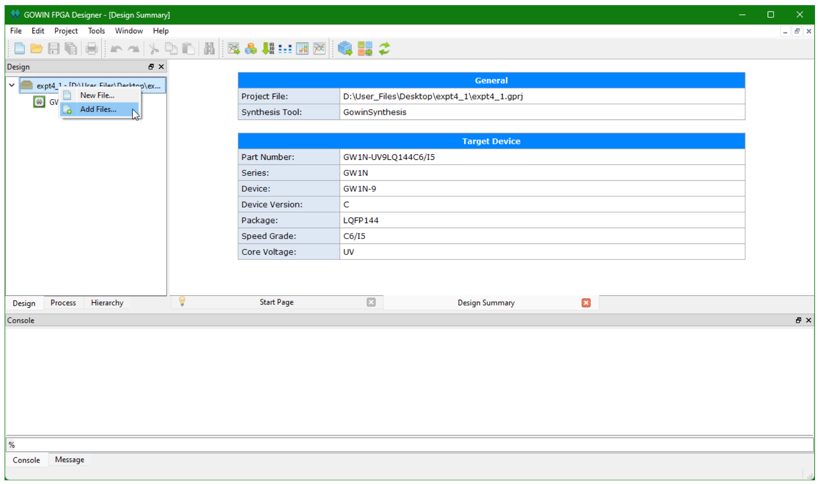
-
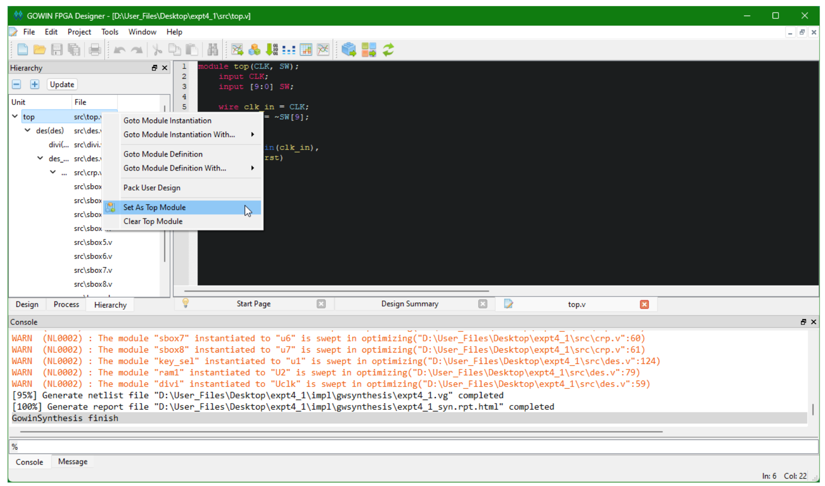
Change the left sidebar to Hierarchy tab. Right click on your top module and select Set As Top Module.
Compiling the FPGA Bitstream
-
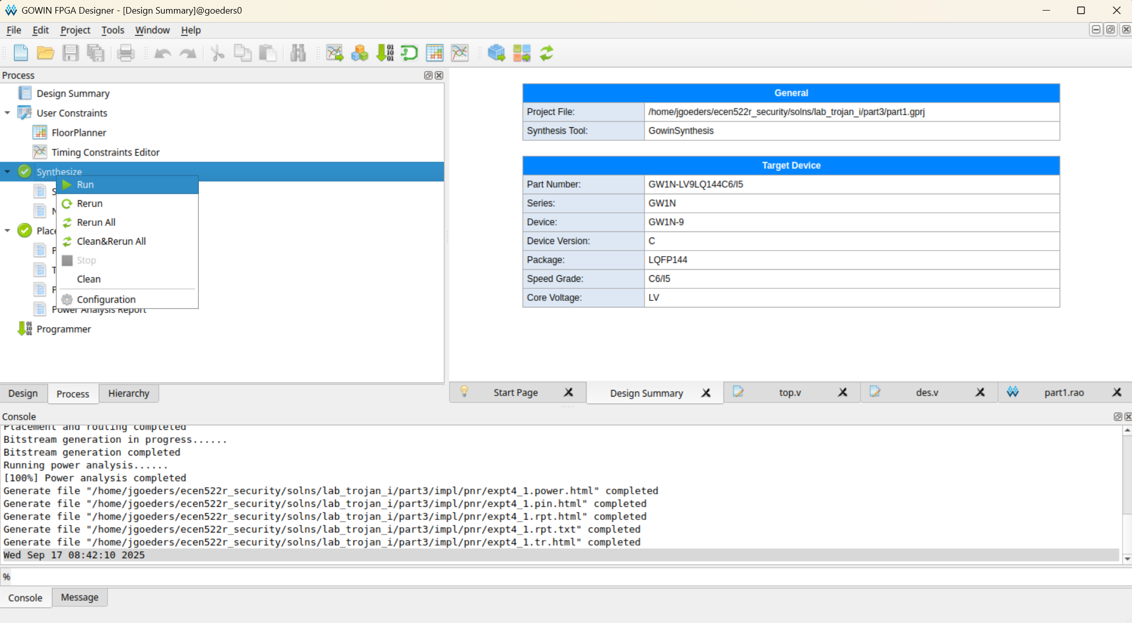
First you must run Synthesis. Run the synthesis tool by changing the left sidebar to Process. Right click on Synthesize and Click Run.
-
Note: If you want to use the Gowin Analyzer Oscilloscope (GAO) to view internal signals on the FPGA, you need to set that up now before proceeding. See the next section for instructions on using GAO.
-
Next run Place & Route.
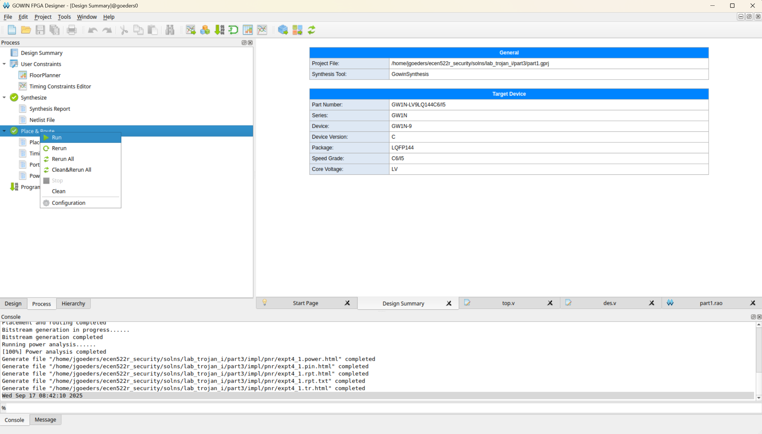
If this succeeds, you should have a bitstream (
*.fsfile) generated in theimpl/pnrdirectory of your project. -
After Place & Route, you can view the resource usage by opening the Place & Route Report. Within the Resource table, the number of logic elements used is shown as Logic, and the number of flip-flops used is shown as Register.
Programming the FPGA with the Programmer Tool
There are two ways to program the FPGA:
- Using the Programmer tool, or
- from within the GAO tool.
This section describes using the Programmer tool. If you are using the GAO, you can skip this section.
-
Click Tools > Programmer. Make sure the Cable and Port are set to GOWIN USB Cable. If this is not showing up, try the Query/Detect button, and then make sure you ran the
sudo remove_ftdi_serial.shscript (see the Tools page for more details).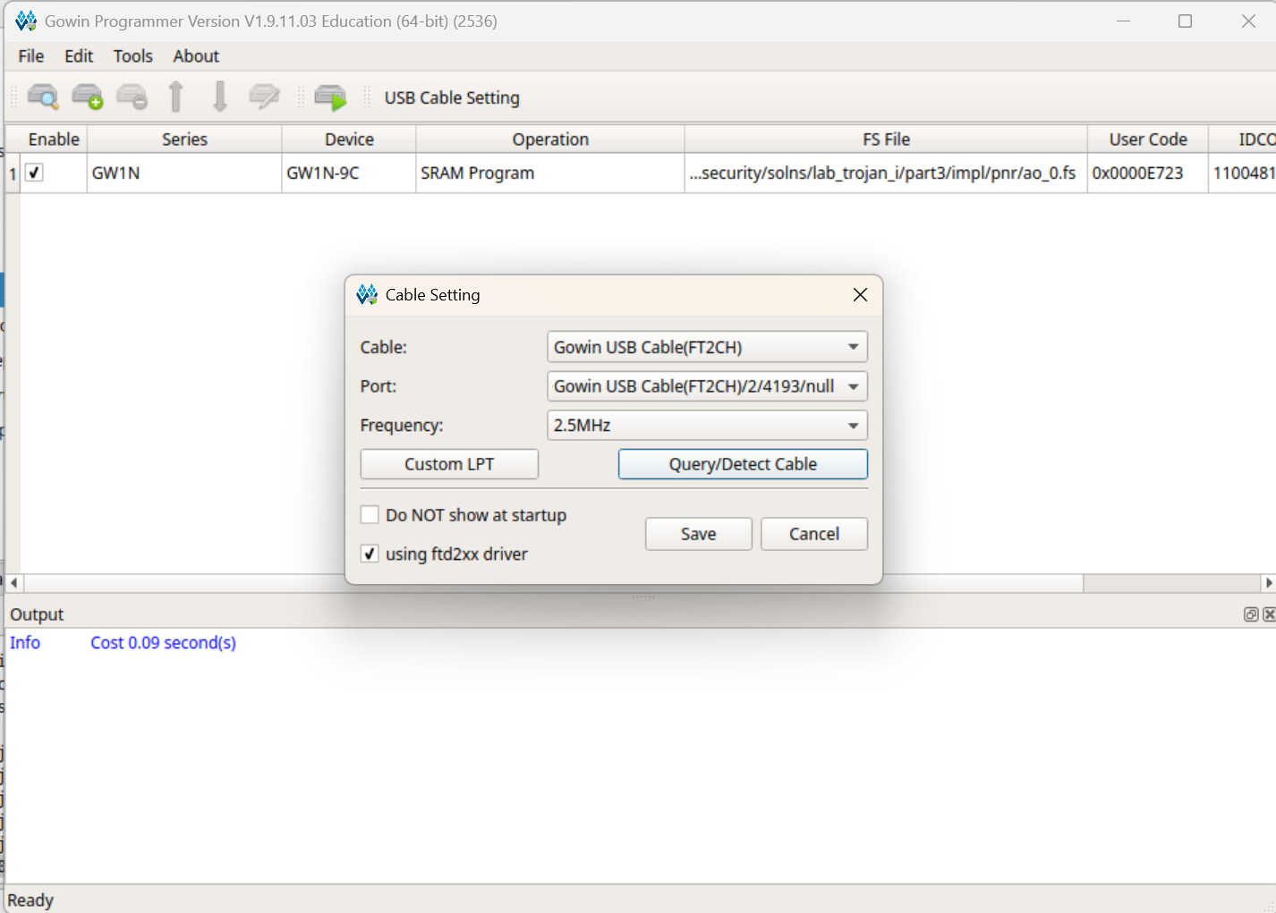
The Gowin Analyzer Oscilloscope (GAO)
The Gowin Analyzer Oscilloscope (GAO) allows you to augment your FPGA design with additional circuitry that can observe and save the values of internal signals to memories on the FPGA. The GAO software tool can then read out these values and display them in a waveform viewer, similar to a traditional logic analyzer. This is very useful for debugging your design, as you can see the internal signals changing in real time.
Using an integrated logic analyzer like the GAO typically involves several steps:
- Synthesizing your design so that the tools can determine what internal signals are available to be observed.
- Configuring the logic analyzer circuitry, which involves:
- Selecting the internal signals you want to observe.
- If triggering mode is used, selecting which signal(s) to use for the trigger condition (we won’t be using this mode in the class).
- Selecting a signal to use as the clock for capturing data. This will determine how often data is captured. Remember, on-chip memories are small, so you won’t be able to capture very many samples of data. If you use a clock must faster than your data is changing, you will just see the same data repeatedly.
- Completing the FPGA compilation process and generating a bitstream with the logic analyzer circuitry included.
- Programming the FPGA with the bitstream.
- Using the logic analyzer software to communicate with the logic analyzer circuitry on the FPGA, instruct it to capture data, retrieve the data from the on-chip memories, and finally, display it in a waveform viewer. Like a traditional logic analyzer or oscilloscope, you capture data in different modes:
- Single: Capture data once when you manually trigger it.
- Auto: Continuously capture data, and display the most recent capture.
- Trigger: Set a trigger condition, and capture data when the trigger condition is met. This is more advanced, and we don’t provide instructions on how to use this mode in the class.
Configuring the GAO
- Create a new file with type GAO Config File. Click OK.
-
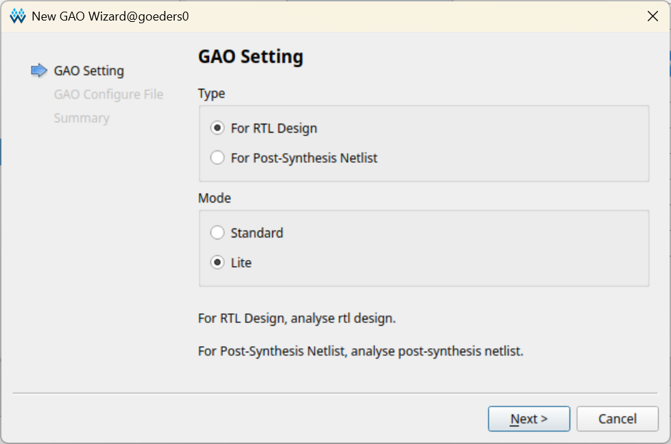
Select For RTL Design and Lite mode. This will disable the trigger mode.
-
Select a name for the configuration file, save it in your src directory, and click Add to current project. Click Finish.
-
In the Design tab, locate your
.raofile, and double click it to open it.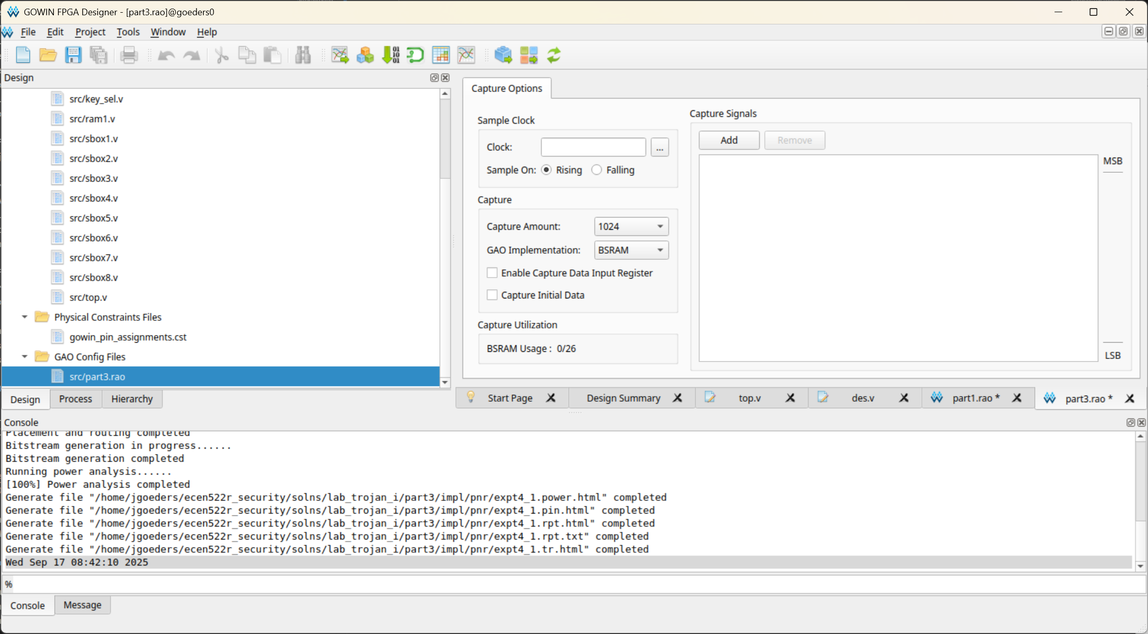
-
Find a signal in your design to use as the clock for capturing data. Click the
...button next to Sample Clock, and in the pop-up box, search for a signal by name.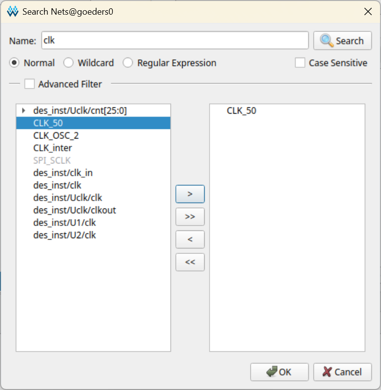
Select the signal you want to use, click the
>button to move it to the right side, and click OK. If done correctly, you should see the name of the signal in the Clock: field. -
Select the signals you want to observe. Click the Add button, and in the pop-up box, search for signals by name. Select the signal you want to observe, click the
>button to move it to the right side, and click OK. Repeat this step until you have selected all of the signals you want to observe.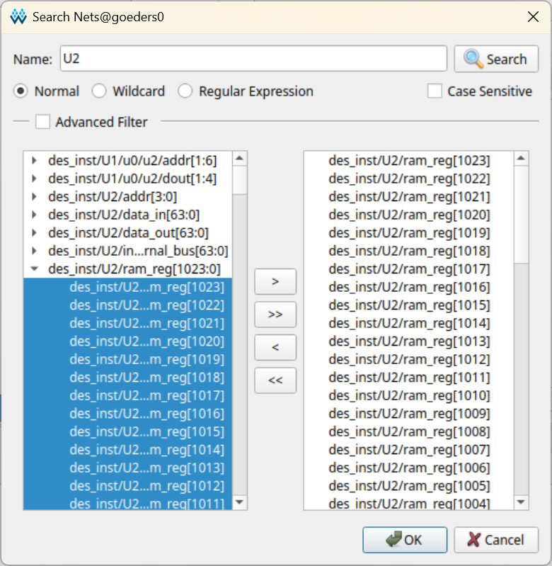
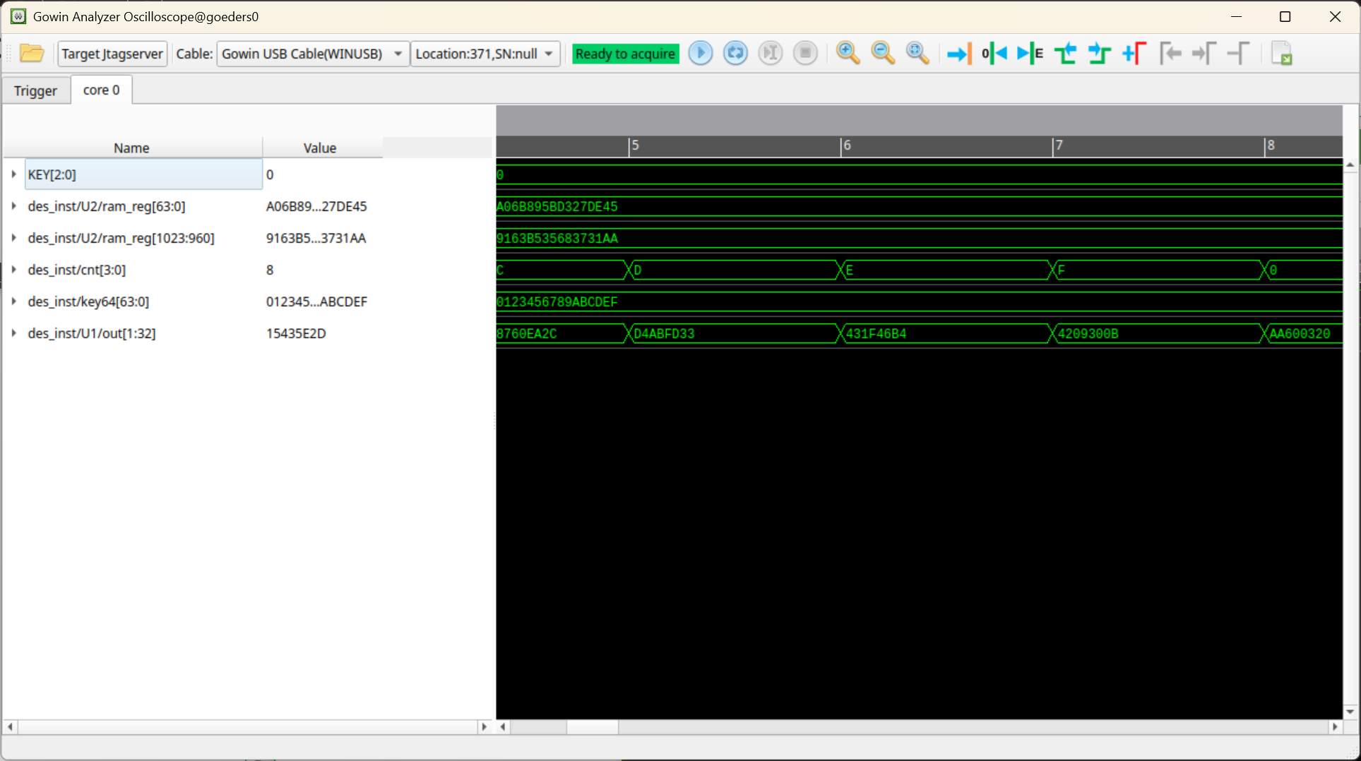
You can select sub-bus signals. For example, in the image above, I am selecting the upper 64 bits of the 1024-bit RAM that stores the results of each round of DES encryption (i.e. the result of the final round).
-
Once back in the GAO configuration window, you can select individual signals, and right-click and click Group, to group them together.
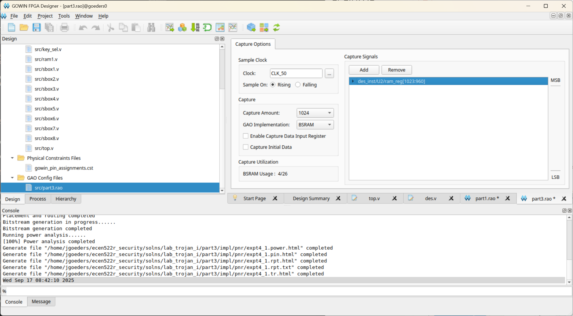
In the image above, I have grouped the upper 64 bits of the RAM together.
- Select the Capture Amount. This is how many clock cycles of data will be captured. Keep an eye on the BSRAM Usage. If you exceed 100%, you will not be able to compile your design, and if you approach 100%, it may take a long time to compile. You can reduce the memory usage by either reducing the Capture Amount, or reducing the number of signals you are observing.
Running the GAO Tool
-
Make sure you have already synthesized your design following the instructions above. This allows the tools to process your Verilog files and determine what internal signals are available to be observed.
-
Run the GAO by clicking Tools > Gowin Analyzer Oscilloscope.
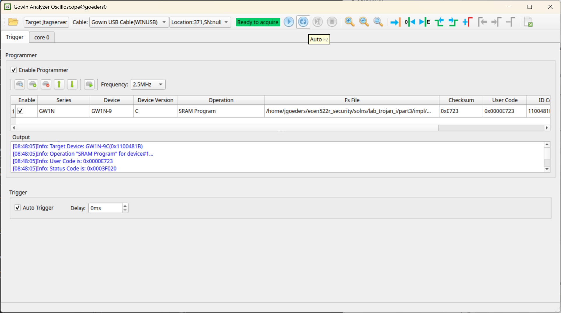
Programming the FPGA
-
Assuming you are programming the FPGA from within the GAO, click the Enable Programmer button. If you already programmed the FPGA using the Programmer tool, you can skip this step.
-
Query the FPGA by clicking the Query Device button. You may need to change the Cable setting at the top. If you don’t see the correct
GW1N-9device listed, try unplugging and replugging the board, and make sure you ran thesudo remove_ftdi_serial.shscript (see the Tools page for more details).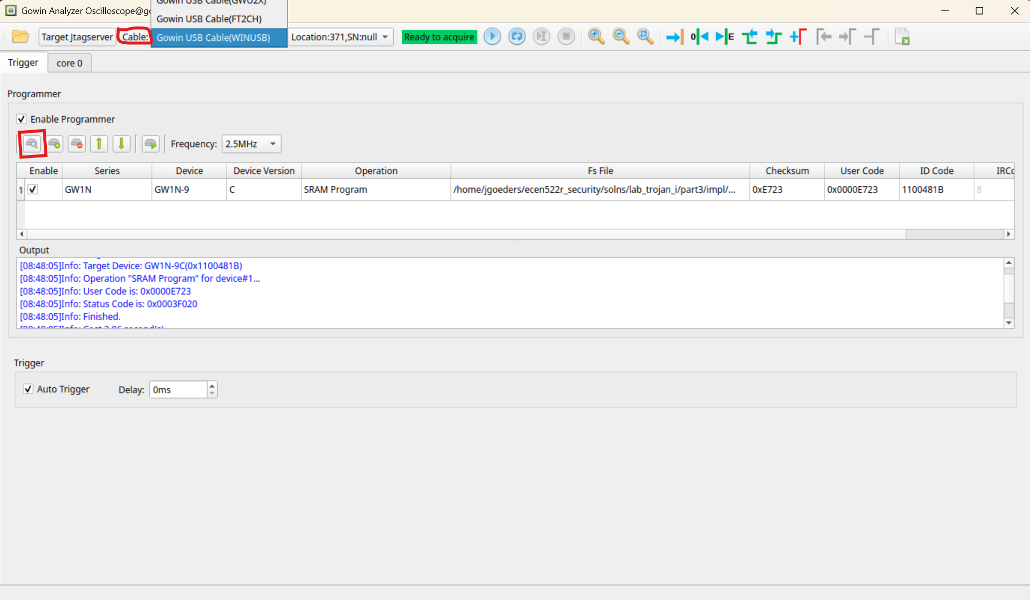
-
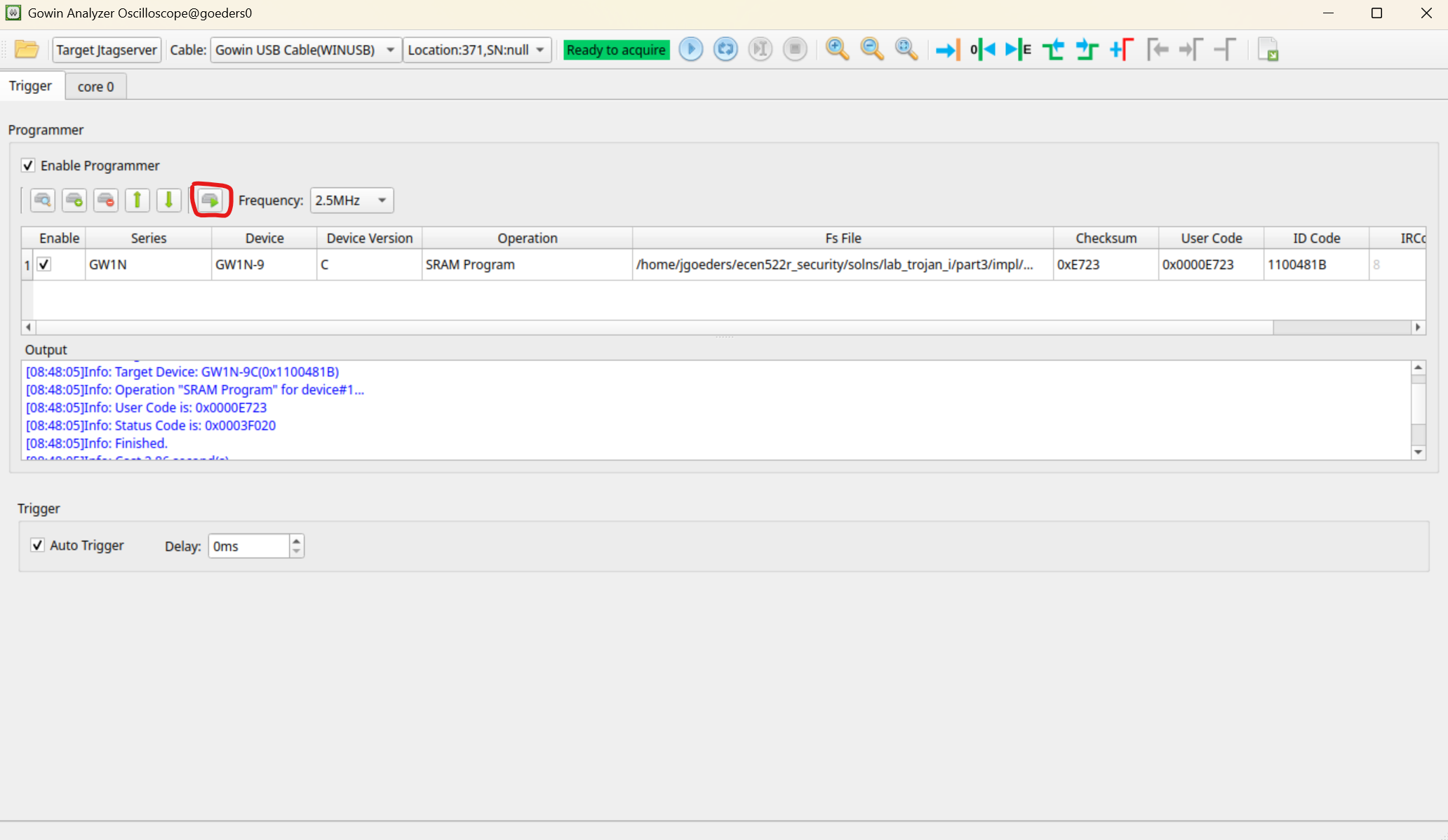
Your bitstream (
*.fsfile) should be automatically detected. If not, click the within the Fs File area and select it from theimpl/pnrdirectory of your project. -
Click the Program button to program the FPGA.
Capturing Data
-
Click the Start button at the top to capture one set of data, as described by the Single mode above.

-
Alternatively, click the Auto button to continuously capture data, as described by the Auto mode above.
-
You should now see the captured data in the waveform viewer. If you selected the Auto mode, you should see the data changing as new data is captured (assuming the signals are changing).