Table of Contents
Lab 7 - RISC-V I/O System
For this laboratory you will integrate your processor into an I/O system and download your processor onto the FPGA board. Your processor will be able to control several I/O interfaces on the FPGA board.
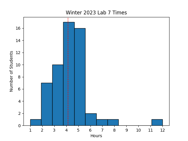 Avg Hours: 5.4, 4.0 (Winter 206, 2022)
Learning Outcomes
- Complete full synthesis and implementation of processor
- Create assembly language programs that run on your RISC-V processor
- Generate a bitstream that could be downloaded onto the FPGA
Preliminary
The RISC-V processor that you have developed over the semester will be inserted into a top-level design that includes other logic that will be provided for you. This logic will allow your processor to interact with the various input/output devices on the FPGA board such as the LEDs and switches. Your processor will be able to control and interact with these devices. A high-level overview of your processor system is shown below:
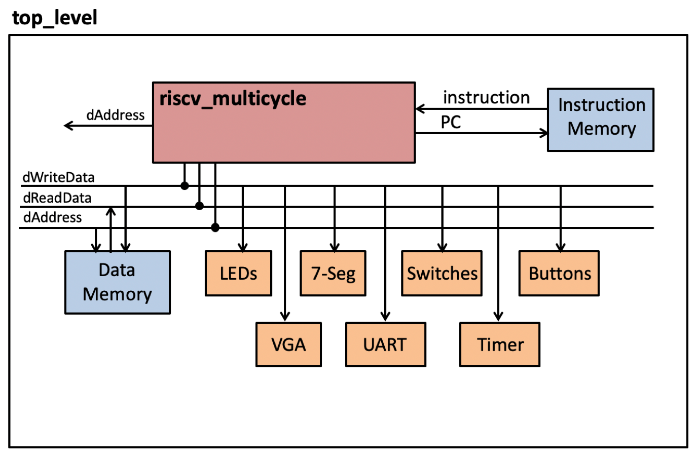
As shown in this figure, the top-level design will include the instruction memory, data memory and a variety of I/O devices. Your RISC-V assembly language programs will be inserted into the instruction memory and the data memory will contain any constants needed by your program and will hold the system stack. In addition to memory, the top-level design includes a variety of I/O devices that your processor can control. These I/O devices include the 16 LEDs, 16 switches, the five buttons, the seven-segment display, the UART, and the VGA display (we will not use the VGA display for this lab). A summary of this I/O system will be provided below in the preliminary and a more detailed description of this system can be found here.
The system that has been created for you has several different address regions, each with a specific and important purpose. It is essential that you understand this address space as you will need to create assembly language programs that properly interact with this system. The purpose of these memory regions is summarized below:
- Instruction Memory (.text): This is the region that contains the instructions of the program that is being executed.
- Data Memory (.data): This is the region that contains the global data memory. The top of this region is used for the stack and the bottom of this region is used for global data memory.
- Memory Mapped IO (mmio): This region is allocated for specific I/O devices such as the LEDs. The memory mapping of these devices and the control of these devices will be explained in detail below.
- Memory Mapped VGA Display (vga): This region is allocated for the VGA character display. The mapping of this memory space to actual VGA locations will be described in a later lab.
The address range and size of each of these memory regions is summarized below:
| Address Range | Size (bytes) | Purpose |
|---|---|---|
| 0x00000000 - 0x00001fff | 8192 | Instruction Memory (.text) |
| 0x00002000 - 0x00003fff | 8192 | Data Memory (.data) |
| 0x00007f00 - 0x00007fff | 256 | Memory Mapped I/O |
| 0x00008000 - 0x0000bfff | 16384 | VGA Space |
Match addresses with the appropriate memory region.
Memory Mapped I/O
The I/O devices that have been added to this system can be controlled and monitored by writing data to and reading data from reserved memory locations that are dedicated to I/O devices in the system. This approach for controlling I/O is called “Memory Mapped I/O”. Memory Mapped I/O includes dedicated decoding logic within that monitors the address and control signals coming out of the RISC-V processor. When this decoding logic observes a write operation (caused by the ‘sw’ instruction) at the specific location of a I/O device, it intercepts this write and sends the data to the appropriate I/O device. The I/O devices act just like a memory in that they accept data from the ‘sw’ instruction and provide data back to the processor from the ‘lw’ instruction.
256 bytes of address space has been reserved for the I/O devices in this system. The I/O space is located at 0x0000_7f00 (i.e., 0x0000_7f00 - 0x0000_7fff). To access the I/O memory, you will need to load a register with the base address of the I/O memory space (0x0000_7f00).
Each individual I/O device in this system has a specific address reserved within this range and is represented as an 8-bit address. For example, the I/O device with an offset of 0x18 is located at 0x000_7f18. The I/O space reserved for the system you are using is summarized in the table below:
| I/O Offset | Read | Write |
|---|---|---|
| 0x00 (0) | Read value of LEDs | Write LED values |
| 0x04 (4) | Read Switch status | N/A |
| 0x18 (24) | Seven Segment Display Value | Seven Segment Display Value |
| 0x24 (36) | Read Buttons status | N/A |
| 0x30 (48) | Timer (ms) | New Timer value |
The function of each of these I/O devices and how they are mapped to this I/O address space will be described below. Several assembly language code examples will be given to demonstrate how to use these I/O devices.
I/O Base Address
To access the I/O memory, you will need to load a register with the base address of the I/O memory space (0x0000_7f00).
If we had access to the full RISC-V instruction space, we could simply use a lui instruction followed by a addi instruction to load a register with this address (i.e., the li pseudo instruction).
Unfortunately we do not have access to this instruction at this point (we will add it later in the semester) and we will need to initialize a register with this address in a more awkward way.
The approach shown below will initialize register x3 by loading 0x7f into x3 and then “shifting” x3 to the left 8 places.
    # Loading 0x7f into x3
    addi x3, x0, 0x7f
    # Shift x3 8 times
    slli x3, x3, 8
    # x3 should have 0x7f00
At this point, x3 should have the base address of the I/O address space and you can use this register to access the I/O modules described below. All of the code examples shown below assume that this base address is stored in register x3.
LEDs
Your RISC-V processor is able to control the 16 LEDs that are provided on the Basys 3 board. You can turn these LEDs on by writing data to address 0x0000_7f00 (0x0000_7f00 + 0). Writing to this memory location using a store word (‘sw’) instruction will set the value of the 16 LEDs. Bit 0 of the word corresponds to LED 0, bit 1 corresponds to LED 1, and so on. Note that since there are 16 LEDs and 32 bits in a word, the upper 16 bits written to this address location will be ignored. The bit value ‘1’ corresponds with turning ‘on’ the corresponding LED.
The following code example demonstrates how to write the value 0xa5 to the LED registers.
    # Assumes that x3 contains the I/O address space
    .eqv LED_OFFSET 0x0
    addi x6, x0, 0xa5
    sw x6, LED_OFFSET(x3)
This example will turn ON the following LEDs: LED7, LED5, LED2, and LED0. All other LEDs will be turned off.
What is the 16-bit value that should be used to turn ON the following LEDs: LED14, LED13, LED10, LED5, LED4, LED2, and LED1.
Note that you can also read from this memory location using the load word (‘lw’) instruction to determine which LEDs are currently turned on (as dictated by a previous ‘sw’ instruction to the LEDs).
Switches
The memory mapped address 0x0000_7f04 (0x0000_7f00 + 0x04) corresponds to the slide switches. Reading from this memory location will indicate which switches are in the “on” (up) position. Bit 0 of the resulting word corresponds to the status of SW0 (right-most switch), bit 1 corresponds to SW1, and so on. Since there are only 16 switches, the top 16 bits of this word will always be zero. Writing a value to this memory location will not do anything. The following code example demonstrates how to read the switches:
    # Read the switches from 0x00007f04 by providing an offset of 4 to t0
    # (t0 + 4 = 0x00007f04)
    .eqv SWITCH_OFFSET 0x4
    lw t1, SWITCH_OFFSET(x3)
    # The value of the switches is now in t1
Indicate what the following Example #1 assembly language program will do?
    # Example #1
    lw t1, 4(x3)
    xori t1, t1, -1
    sw t1, 0(x3)
Buttons
The address 0x0000_7f24 (0x0000_7f00 + 0x24) corresponds to the push buttons. Reading from this memory location will indicate buttons which are pressed. When a button is pressed, the bit corresponding to the button will have the value ‘1’. The relationship between bit location and button is summarized in the table below:
| 4 | 3 | 2 | 1 | 0 |
|---|---|---|---|---|
| UP | RIGHT | DOWN | LEFT | CENTER |
| BTNU | BTNR | BTND | BTNL | BTNC |
The following example demonstrates how to read the buttons, branch back when the ‘down’ button (BTND) NOT pressed, and then fall through when the ‘down’ button IS pressed:
    # It is better to use constants when programming I/O
    .eqv BUTTON_OFFSET 0x24
    .eqv BUTTON_D_MASK 0x04
    # Assume x3 has the I/O base address
wait_for_btnd:
    # Read the buttons
    lw t1, BUTTON_OFFSET(x3)
    # Mask the buttons for button D
    andi t1, t1, BUTTON_D_MASK
    # If button d is not pressed, branch back
    beq t1, x0, wait_for_btnd:
button_d_pressed:
    # fall through after button d is pressed
Determine what the following Example #2 code sequence does.
    # Example #2
    .eqv BUTTON_OFFSET 0x24
    .eqv BUTTON_D_MASK 0x04
L1:
    lw t1, BUTTON_OFFSET(x3)
    andi t1, t1, BUTTON_D_MASK
    beq t1, x0, L1
L2:
    lw t1, BUTTON_OFFSET(x3)
    andi t1, t1, BUTTON_D_MASK
    xori t1, t1, -1
    andi t1, t1, BUTTON_D_MASK
    beq t1, x0, L2
L3:
Seven-Segment Display
Address 0x0000_7f18 (0x0000_7f00 + 0x18) corresponds to the seven-segment display. Writing to this memory location will cause the lower 16-bits of the word being written to at this address to be displayed in hex on the four digits of the seven segment display. Like the LEDs, you can read the value of this memory location to see what value is currently being displayed on the seven-segment display. The following code segment demonstrates a loop that continuously updates the value of the seven segment display:
    .eqv SEVEN_SEGMENT_DISPLAY_OFFSET 0x18
    addi t1, x0, 0
loop:
    sw t1, SEVEN_SEGMENT_DISPLAY(x3)
    addi t1, t1, 1
    beq x0, x0, loop
Determine what the following Example #3 code sequence does.
    # Example #3
    .eqv BUTTON_OFFSET 0x24
    .eqv BUTTON_D_MASK 0x04
    .eqv SEVEN_SEGMENT_DISPLAY_OFFSET 0x18
    addi t2, x0, 0
L1:
    lw t1, BUTTON_OFFSET(x3)
    andi t1, t1, BUTTON_D_MASK
    beq t1, x0, L1
L2:
    sw t2, SEVEN_SEGMENT_DISPLAY(x3)
    addi t2, t2, 1
    beq x0, x0, L1
Timer
A simple timer has been added to the system to provide a time stamp to facilitate timing accurate interactions. When the timer is read (0x0000_7f30), it will return the number of milliseconds since the processor was first turned on or since it was last reset. The timer can be loaded with any value by writing to the same address location (this is a convenient way to reset the timer). The following code example demonstrates how to wait for 10 ms:
    .eqv TIMER 0x30
    sw x0, TIMER(x3)      # Clear timer to zero
    addi t1, x0, 10       # Set t1 to 10 (10 milliseconds)
wait:
    lw t2, TIMER(x3)
    beq t2, t1, after_wait
    beq x0, x0, wait
after_wait:
Determine what the following Example #4 code sequence does.
    # Example #4
    .eqv BUTTON_OFFSET 0x24
    .eqv BUTTON_D_MASK 0x04
    .eqv SEVEN_SEGMENT_DISPLAY_OFFSET 0x18
    .eqv TIMER 0x30
    addi t3, x0, 0
    sw t3, SEVEN_SEGMENT_DISPLAY(x3)
    addi t1, x0, 500
L1:
    lw t0, BUTTON_OFFSET(x3)
    andi t0, t0, BUTTON_D_MASK
    beq t0, x0, L1
L2:
    sw x0, TIMER(x3)
L3:
    lw t2, TIMER(x3)
    beq t2, t1, L4
    beq x0, x0, L3
L4:
    addi t3, t3, 1
    sw t3, SEVEN_SEGMENT_DISPLAY(x3)
    beq x0, x0, L2
The I/O sub-system also includes the UART and the VGA controller but these will be not be used in this lab (they are described here and will be used in a future lab).
Exercises
Before proceeding with your laboratory exercises, update your repository with the latest lab starter code.
Exercise #1 - I/O System TCL Simulation
In this first exercise you will simulate your processor from the previous lab executing within the I/O system described above.
A set of SystemVerilog files has been created that implements the I/O functions described above.
You will insert your multi-cycle processor into this system to provide your processor with the memories and I/O you need.
A simple test I/O program, multicycle_iosystem.s, has been written that operates on the I/O system described above.
This program uses the buttons, switches, LEDs, and seven-segment display.
Carefully review this program and answer the questions on Learning Suite about its functionality.
Answer the questions about the test program in Learning Suite
A makefile fragment file named multicycle_iosystem.mk has been provided for you to provide the makefile rules need to simulate the multicycle iosystem in Vivado as well as generate a bitfile for the system.
Add the line include multicycle_iosystem.mk at the top of your makefile to inherit the makefile rules in your makefile.
Also, add the dependency clean-iosystem to your clean: rule in your makefile.
This dependency will call the clean-iosystem rule in multicycle_iosystem.mk to clean the iosystem build files.
This makefile includes another makefile fragment ../resources/iosystem/iosystem.mk which includes a generic rule for generating .mem files from .s files.
Running make multicycle_iosystem_text.mem will generate the text memory files from the multicycle_iosystem.s assembly language program.
Run the makefile rule sim_multicycle_iosystem_tcl_template to simulate your processor within the I/O system with the assembly language program.
When simulating this system with the precompiled program, you will receive messages indicating reads and writes to the I/O ports.
The following example demonstrates the output of this simulation:
Reset released at time 530000
890000:Writing 0x00000000 to Seven Segment Display
1040000:Writing 0x00000000 to Timer
1220000:Reading 0x00000000 from Buttons
1370000:Reading 0x00000000 from Switches
1820000:Reading 0x00000000 from Timer
1940000:Writing 0x00000000 to Seven Segment Display
3440000:Writing 0x00000000 to LEDs
3770000:Reading 0x00000000 from Buttons
3920000:Reading 0x00000000 from Switches
4370000:Reading 0x00000000 from Timer
4490000:Writing 0x00000000 to Seven Segment Display
5990000:Writing 0x00000000 to LEDs
Once you have successfully simulated the template .tcl file, create your own iosystem.tcl file by copying the iosystem_template.tcl file and adding additional stimulus to this file to simulate the various buttons and switches.
Specifically, add the following stimulus to the iosystem.tcl file to simulate button presses and switch changes:
- Change the value of the switches, observe impact on LEDs
- Press BTNU, observe impact on LEDs
- Press BTNR, observe impact on LEDs
- Press BTNL, observe impact on LEDs
- Press BTND, observe impact on LEDs
- Simulate at least 1 ms to see the timer reach a value of 1 ms
- Press BTNC and observe the impact on the timer and seven segment display Note that when you simulate a button press, you need to hold the value of the button for about 4 us so that it is high long enough for the code to detect the button press.
There is a makefile rule named sim_multicycle_iosystem_tcl that will simulate the iosystem.tcl file you create.
Run this rule to make sure your processor simulates properly with your .tcl file.
You will need to include this .tcl file as part of your lab submission
Exercise #2 - Testbench Simulation
After convincing yourself that your processor is hooked up properly and that the program you have been given is working, you will need to test your processor with a testbench.
The makefile contains a makefile rule named sim_multicycle_iosystem to run your processor with a testbench.
Make sure your design passes this testbench simulation before proceeding to the next exercise.
Answer the following questions about the testbench in Learning Suite
At what time do the LEDs first change from all zeros to a non-zerio value? Provide your answer in decimal microseconds (us)
At what time do the LEDs change back to all zeros from a non-zerio value?
At what time do the LEDs change to 0xffff (i.e., all on)?
Exercise #3 - Synthesize, Implement, and Generate Bitstream
For this exercise, you will synthesize, implement, and download your processor along with the I/O sub-system precompiled with the demonstration program.
A constraints file has been created for you that maps the top-level I/O signals to the pins on the BASYS3 board.
The makefile rule multicycle_iosystem.bit will perform the synthesis, implementation, and bitstream generation for the system with the demonstration program.
Review the implement_multicycle_iosystem.tcl implementation script to see how the synthesis and implementation steps are performed for this design.
Summarize the estimated resources for your implemented design. Use the ‘utilization report’ for your responses (not synthesis report).
| Resource | Estimation |
|---|---|
| LUT* | |
| RAM?32 | |
| FD* | |
| RAMB* | |
| IBUF+OBUF | |
| BUFG | |
| MMCM* |
Determine the ‘Worst Negative Slack’ (WNS) for your design (see timing report).
Download
Download the bitstream to the Basys3 board and verify that it operates as you expect. Although this bitstream will not be tested during the passoff script, you are strongly encouraged to test this design on your board to make sure it works. If it does not work, resolve any problems before proceeding to the next exercise.
Exercise #4 - Custom Program
For this final exercise, you will create your own program that runs on your multi-cycle RISC-V processor.
Create a new assembly language program named buttoncount.s that performs the same buttoncount functions you implemented in the first lab.
Specifically, your program should perform the following functions:
- Increment the LEDs by 1 when BTNU is pressed
- Decrement the LEDs by 1 when BTND is pressed
- Clear the LEDs when BTNC is pressed.
- Increment the LEDs by the value indicated by the switches when BTNL is pressed.
- Decrement the LEDs by the value indicated by the switches when BTNR is pressed.
- Note that the switches are considered “signed” values so you will need to sign extend the 16-bit switch values to 32-bits before performing the increment/decrement functions for BTNL and BTNR. In addition to the button counting functions, your program should also continuously update the seven-segment display with the value of the timer. Every time a button is pressed, the timer should be reset to zero so that the seven-segment display will show the number of milliseconds (in hex) since the last button was pressed.
Note: You need to implement “one shot” functionality in your program to make sure that you only increment/decrement when the button is first pressed. This can be done in software by creating a section of code that loops to check for the initial pressing any of the three buttons.
Use the file multicycle_iosystem.s as a start for your code (i.e., copy it to a filed named buttoncount.s)
Follow the assembly language coding standard as you write your assembly language code.
After you have created your assembly language program, assemble the program into a hex memory dump file named buttoncount_text.mem.
There already is a rule for converting .s files into _text.mem files so running make buttoncount_text.mem will generate this file.
A simulation tcl file named buttoncount.tcl has been created for you to stimulate the switches and buttons in your program.
Use this stimulus to make sure your program is operating properly.
After you have verified that your program operates correctly, add a makefile rule named multicycle_buttoncount.bit that will generate a bitfile with the same name using your buttoncount memory file.
You will need to create a custom implementation ‘tcl’ script that provides a different memory file for the TEXT_MEM parameter in the synth_design command (see the implement_multicycle_iosystem.tcl as an example).
Note: Make sure you test the bitstream generated through this process on your board. The TAs will build and run your bitstream to make sure it works. You will lose significant points on this lab if your generated bitstream does not operate correctly.
Pass Off
The final step in the laboratory process is to complete the ‘pass off’. Carefully review the instructions for Git Submission as you prepare your submission for this lab. You will need to run the following command successfully to submit your lab:
python3 passoff.py --submit
Include the following information at the end of your laboratory report.
How many hours did you work on the lab?
Provide any suggestions for improving this lab in the future
How did you use AI to help you with this lab