Table of Contents
Lab 6 - RISC-V Control
For this laboratory you will design the control unit for a simplified, multi-cycle, non-pipelined datapath you designed in the previous laboratory. Your simple RISC-V processor will be able to execute simple assembly language programs.
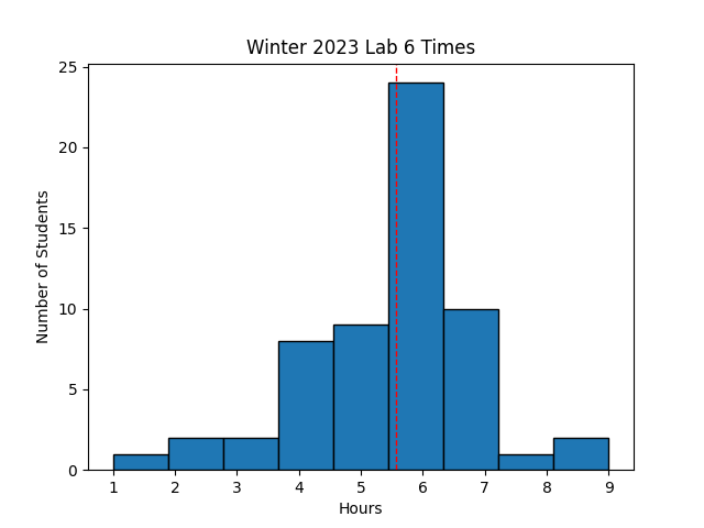 Avg Hours: 6.3, 6.4, 5.6 (Winter 2026, 2022, Winter 2021)
Learning Outcomes
- Implement a multi-cycle control unit for the RISC-V datapath in SystemVerilog
- Verify the control unit of the RISC-V processor by executing a simple program
Preliminary
A simple single-cycle control implementation of the RISC-V processor is described in detail in Sections 4.4 (pages 269-283) of the textbook. You will need to understand this section of the book in great detail to complete this lab. You will likely need to refer to these sections of the textbook as you complete this lab. Make sure you have access to your textbook while completing this lab. You will be creating a controller for your datapath to implement the following 21 instructions:
| Type | Instruction |
|---|---|
| Arithmetic/Logic | add, sub, slt, sll, srl, sra |
| Arithmetic/Logic Immediate | addi, slti, slli, srli, srai |
| Logical | and, or, xor |
| Logical Immediate | andi, ori, xori |
| Branch | beq |
| Memory | lw, sw |
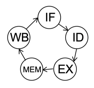
For this lab, you will be creating a multi-cycle controller that executes each instruction in five clock cycles. You will implement a state machine that sequences between the following five states for instruction execution:
| State | Purpose |
|---|---|
| IF | Instruction fetch: provide the PC to the instruction memory |
| ID | Instruction Decode: decode the received instruction and start register access |
| EX | Execute: execute the operation in the ALU |
| MEM | Memory: perform memory access (for ld/sd) |
| WB | Write Back: write new data into register file |
A state diagram demonstrating these instruction steps is shown below:
The primary purpose of this lab is to implement the state machine and generate the control signals for the datapath unit. The following discussion and set of questions will help you understand the logic you need to create the control signals.
ALUCtrl
‘ALUCtrl’ is a four-bit control signal that dictates the operation of the ALU. As described in the book and in the class lecture, generating the ‘ALUCtrl’ signal requires multi-level decoding involving the ‘opcode’ field of an instruction as well as the ‘funct3’ and ‘funct7’ bits. The decoding logic should set the ALU operation based on the instruction as follows:
- load and store: addition
- branch: subtraction
- ALU operations: operation based on funct3 and funct7 (including shift instructions)
To test your understanding of the decoding necessary for this signal, determine the value of the ALUCtrl signal for each of the following instructions:
| 32-bit instruction | ALUCtrl |
|---|---|
| 0x004b2283 | 0010 |
| 0x403100b3 | |
| 0x0ff0c193 | |
| 0x04510463 | |
| 0x01830493 | |
| 0x0078e533 | |
| 0x0062a233 | |
| 0x0028a623 | |
| 0x01d3f2b3 | |
| 0x00350533 | |
| 0x0163f293 | |
| 0x0ff9a693 |
ALUCSrc
When ‘ALUSrc’== 0, the register read 2 output is used as the input to operand 2 of the ALU. When ‘ALUSrc’== 1, immediate data for the input to operand 2 of the ALU (see Figure 4.19 in the text). Immediate data is needed for ‘load’, ‘store’, and ‘ALU Immediate’ instructions. You can determine the value of ‘ALUSrc’ directly from the opcode bits of the instruction.
Determine the value of the ‘ALUSrc’ signal for each of the following instructions (for instructions in which it doesn’t matter, enter a ‘0’ or a ‘1’).
| 32-bit instruction | ALUSrc |
|---|---|
| 0x004b2283 | 1 |
| 0x403100b3 | |
| 0x0ff0c193 | |
| 0x04510463 | |
| 0x01830493 | |
| 0x0078e533 | |
| 0x0062a233 | |
| 0x0028a623 | |
| 0x01d3f2b3 | |
| 0x00350533 | |
| 0x0163f293 | |
| 0x0ff9a693 |
MemRead and MemWrite
Two signals control the memory interface: ‘MemRead’ and ‘MemWrite’. The ‘MemRead’ signal is set for ‘load’ instructions and the ‘MemWrite’ signal is set for ‘store’ instructions. Unlike the previous signals, these signals should only be set during the ‘MEM’ stage of the instruction state machine.
Determine which of the following instructions should set the ‘MemRead’ signal and ‘MemWrite’ signals during the ‘MEM’ instruction stage:
(0x004b2283, 0x403100b3, 0x0ff0c193, 0x04510463, 0x01830493, 0x0078e533, 0x0062a233, 0x0028a623, 0x01d3f2b3, 0x01d3f2b3, 0x00350533).
MemtoReg and RegWrite
The ‘RegWrite’ signal is used to control when values are written to the register file. For this five-cycle execution sequence, ‘RegWrite’ should only be set to ‘1’ during the ‘WB’ state of the instruction state machine. Some instructions do not write back to the register file so this signal will stay low for the entire five clock cycle instruction sequence.
The ‘MemtoReg’ signal is based on the current instruction and is set to ‘1’ only when executing a ‘load’ instruction. This signal does not depend on the current state (it doesn’t matter what this signal is during all state except the ‘WB’ state).
Determine which instructions should set the ‘RegWrite’ signals during the ‘WB’ instruction stage.
loadPC and PCSrc
The ‘loadPC’ signal is used to update the PC with a new value. The ‘loadPC’ signal should be set to ‘1’ during the ‘WriteBack’ state of every instruction (thus loading a new PC value before entering the next IF state).
The ‘PCSrc’ signal is used to indicate which value to load to the PC: ether PC+4 for regular instructions or PC+branch_offset for branch taken operations. This signal is based on both the current instruction and on the value of the ‘Zero’ signal. This signal should be set to ‘1’ when the following conditions are present: (1) current instruction is a “BEQ” function, and (2) the Zero flag is high.
Assuming the Zero flag is high, determine which of the following instructions should set the ‘PCSrc’ signal to ‘1’.
Exercises
Before proceeding with your laboratory exercises, update your repository with the latest lab starter code.
Exercise #1 - Verilog RISC-V Processor
For this exercise you will implement the basic RISC-V processor as described in the textbook.
Begin your exercise by creating an empty Verilog module named riscv_multicycle.sv with the following top-level ports.
| Module Name: riscv_multicycle | |||
|---|---|---|---|
| Parameter | Width | Default Value | |
| INITIAL_PC | 32 | 0x00400000 |
| Port Name | Direction | Width | Function |
|---|---|---|---|
| clk | Input | 1 | Global clock |
| rst | Input | 1 | Synchronous Reset |
| instruction | Input | 32 | Instruction data from Instruction Memory |
| dReadData | Input | 32 | Data read from data memory |
| PC | Output | 32 | Program Counter |
| dAddress | Output | 32 | Address for data Memory |
| dWriteData | Output | 32 | Data to write into data memory |
| MemRead | Output | 1 | Control signal indicating memory read |
| MemWrite | Output | 1 | Control signal indicating memory write |
| WriteBackData | Output | 32 | Data being written to registers (for debug) |
Like the datapath module in the previous lab, your module should have a parameter for the INITIAL_PC. The following steps will guide you through the process of creating this module.
1. Datapath
The first step is to instance the datapath circuit you created in the previous lab. When you instance your datapath circuit, you should pass the INITIAL_PC parameter of this module to your datapath module. This parameter indicates the initial value in memory where your ‘.text’ segment will execute. The organization of the datapath circuit in relation to the control logic and the top-level ports is shown in the figure below:
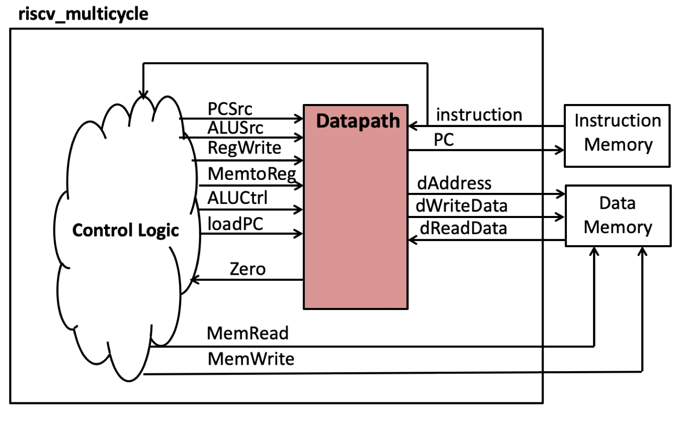
Attach the following ports in the datapath module to their corresponding top-level port within this new module:
- PC
- instruction
- dAddress
- dReadData
- dWriteData
The rest of the logic within this module will generate the control signals that control the datapath module and will be described in more detail below.
2. State Machine
Create a five-state state machine that sequences through the following five steps of executing an instruction:
- IF: Instruction Fetch
- ID: Instruction Decode
- EX: Execute
- MEM: Memory Access
- WB: Write Back
The state diagram for this state machine is shown below. The state machine should return to the ‘IF’ state when the synchronous reset is provided.
3. Control Signals
With the state machine created, create the control signals that will control the datapath.
- The signals
ALUSrc,ALUCtrl, andMemtoReg, depend on the current instruction value only. You do not need to use the current processor state to set these signals. - The
PCSrcdepends on the current instruction and thezerosignal. It also does not need to use the current processor state. - The signals
RegWrite,MemRead, andMemWriteshould only be asserted during the appropriate processor state. - The
loadPCdepends only on the current processor state (it operates the same for all processor instructions).
As you create the logic for your controller, you may need additional constants in your SystemVerilog code.
If additional constants are needed, add them to the riscv_datapath_constants.sv file in the include directory of your project.
Exercise #2 - Testbench Simulation
For this exercise, you will simulate your multicycle processor using a testbench that uses the simple_datapath.s test program used in the previous lab.
The testbench is named tb_multicycle.sv and requires a number of files to properly execute.
Create a makefile rule named sim_tb_multicycle to run your test bench.
Implement the following in your makefile to create the testbench:
- Generate the
simple_datapath_text.memandsimple_datapath_data.memmemory files from thesimple_datapath.sin lab 5. - Generate a log file named
sim_tb_multicycle.log. - Add the
--include ../includeflag toxvlogso that the files in the../includedirectory are found - Compile the file
../include/riscv_memory.sv. This is a memory module that will be used for both the instruction and data memories. - Compile the
tb_riscv_pkg.svbefore thetb_multicycle.svfile. - Add the flag
-timescale 1ns/100psto yourxelabcommand for simulation.
Simulate and debug your design until you have no errors in the testbench.
Answer the questions in the lab report concerning the testbench simulation
Exercise #3 - Simple Assembly Program
For this exercise you will write your own assembly language program that runs on your multicycle processor.
This program should be implemented in a file named bounds.s.
Note: When writing this assembly language program make sure you only use the instructions supported by your processor (the instructions listed above).
The data segment for this program starts at 0x0 (“Compact, Data at Address 0” memory model).
The details of the program are as follows:
- A companion file named
bounds_data.sis provided in the starter code. This file contains the test data in the.datasegment that your program will operate on. The details of this file are as follows:- It contains two constants,
MAX_VALUEandMIN_VALUEusing the.eqvdirective that you will need to use in your program. - It contains an array of 32-bit words in the global
.datasegment that you will be checking for “bounds” - The end of the array ends with the value of 0. This value signals the end of the array and you will need to check for it in your program
- It contains two constants,
- Add the statement
.include "bounds_data.s"in yourbounds.sfile. This statement is similar to an include directive in C that will insert thebounds_data.scode into your code. - Create a main function that iterate over each element of the
bounds_dataarray and process each element as follows:- If the value is 0, end your iteration over the array and perform the end of program functions discussed below
- If the value is greater than the
MAX_VALUEconstant, overwrite the data with theMAX_VALUEconstant. In addition, increment thea1register (this register is used to count the number of array elements that are greater thanMAX_VALUE). - If the value is less than the
MIN_VALUEconstant, overwrite the data with theMIN_VALUEconstant. In addition, increment thea2register (this register is used to count the number of array elements that are less thanMIN_VALUE). - After adjusting the array element with either max or min, add the result to the
a0register (this register is used to hold a running count of the adjusted array sum)
- At the end of the program after evaluating each array element, execute the following instructions:
addi x0, a0, 0addi x0, a1, 0addi x0, a2, 0ebreaknop
Simulate your program in the RARS simulator to make sure it is executing properly.
Note: You need to configure the simulator with the “Compact, Data at Address 0” memory configuration when simulating in RARS.
This can be done in the GUI by selecting: Settings->Memory Configuration “Compact, Data at Address 0”.
Review the values of the a0, a1, and a2 registers to confirm your program is executing properly.
After successfully simulating your program in RARS, simulate your program within the tb_multicycle.sv testbench.
Create a makefile rule named sim_tb_multicycle_bounds to run your bounds.s program.
Implement the following in your makefile to create the testbench:
- Generate the files
bounds_text.memandbounds_data.memmemory files from yourbounds.sand the includedbounds_data.sfiles.- Use the
mc CompactDataAtZerooption when generating your files to indicate the memory configuration
- Use the
- When elaborating the
tb_multicyclesimulation model using thexelab, add the following flags:-generic "instruction_memory_filename=bounds_text.mem"This causes the testbench to use the bounds_text.mem file instead of the default filename-generic "data_memory_filename=bounds_data.mem"This causes the testbench to use the bounds_data.mem file instead of the default filename-s tb_multicycle_boundsThis flag indicates that the simulation should be namedtb_multicycle_boundsto distinguish it from your previous simulation with the default name oftb_multicycle
- When simulating with the
xsimcommand, use thetb_multicycle_boundsas the argument rather thantb_multicycle(match the-sflag from the elaboration) - Generate a simulation log file named
sim_tb_multicycle_bounds.log.
Exercise #4 - Synthesis
The final exercise in this lab is to synthesize your single-cycle RISC-V control unit in ‘out_of_context’ mode.
Create a makefile rule named riscv_multicycle_synth.dcp that runs this synthesis script.
This rule should generate a synthesis log file named riscv_multicycle_synth.log as well as the design checkpoint file riscv_multicycle_synth.dcp.
You will not be generating a bitfile for this lab, so you do not need to perform the implementation step
Summarize the estimated resources for your synthesized logic in the table below. Note that you will have a warning that you are using too many I/Os. This is ok since we are not downloading a bitstream for this lab.
| Resource | Estimation |
|---|---|
| LUT | |
| RAM32* | |
| FD* |
Pass Off
The final step in the laboratory process is to complete the ‘pass off’. Carefully review the instructions for Git Submission as you prepare your submission for this lab. You will need to run the following command successfully to submit your lab:
python3 passoff.py --submit
Include the following information at the end of your laboratory report.
How many hours did you work on the lab?
Provide any suggestions for improving this lab in the future
How did you use AI to help you with this lab