Table of Contents
Lab #2 - Arithmetic Logic Unit (ALU)
An Arithmetic/Logic Unit or ALU is an important component of any processor system. This unit is the “brains” of the processor and performs the arithmetic functions such as addition and subtraction as well as bitwise logical functions such as AND/OR. You will create an ALU in this laboratory that you will use for your RISC-V processor in a later lab. You will also use this ALU to implement a simple “calculator” on the FPGA.
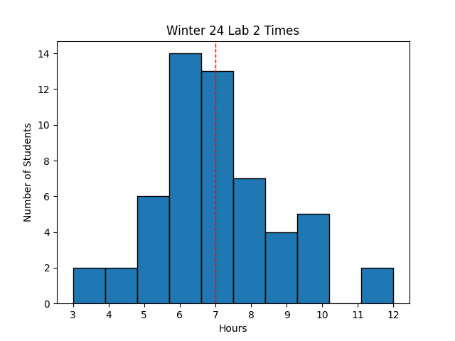 Avg Hours: 5.6, 7.0, 6.9, 6.5, 5.8 (Winter 2026, 2024, 2023, 2022, 2021)
Learning Outcomes
- Apply Hierarchy in a top-level SystemVerilog design
- Create a reusable combinational ALU circuit
- Create top-level ‘calculator’ circuit based on your ALU
- Verify your Calculator circuit with a “testbench” file on the Simulator
Preliminary
The ALU in most processors performs both arithmetic operations (add, subtract, multiply, and divide), bitwise logical operations (and, or, not, xor, etc.), and shift operations (shift right, shift left, etc.). All ALU arithmetic operations are performed in binary arithmetic. You should be familiar with all of these operations from your study in ECEN 320.
For this lab you will be creating the ‘ALU’ for the RISC-V processor. Your ALU will need to implement each of the following operations based on the value of a four-bit control signal named ‘alu_op’. Each of the operands to these operations are 32-bit two’s complement numbers. For ‘alu_op’ values that are not in the table, the ALU should perform an ‘ADD’ operation.
| alu_op | Instruction | Function |
|---|---|---|
| 0000 | AND | Bitwise AND |
| 0001 | OR | Bitwise OR |
| 0010 | ADD | Two’s complement addition |
| 0110 | SUB | Two’s complement subtraction |
| 0111 | SLT | Set less than (return a 1 if op1 < op2 else return 0) |
| 1000 | SRL | shift right logical |
| 1001 | SLL | shift left logical |
| 1010 | SRA | Shift right arithmetic |
| 1101 | XOR | Bitwise Exclusive OR |
The default behavior for values not specified is addition1. In addition to the 32-bit ALU output, your ALU module will need to provide a single-bit output that indicates when the ALU result is zero.
Assuming ‘op1’=32’hf3212f37 and ‘op2’=32’h621c3ee7, determine the value of ALU result for the given value of ‘alu_op’:
- 4'b0000
- 4'b0001
- 4'b0010
- 4'b0011
- 4'b0110
- 4'b0111
- 4'b1000
- 4'b1001
- 4'b1010
- 4'b1101
Exercises
Before proceeding with your laboratory exercises, update your repository with the latest lab starter code.
Exercise #1 - Arithmetic and Logic Unit
Begin your ALU module by creating a new SystemVerilog file named alu.sv.
Define the module named alu and add the following ports (the port names MUST be exact to match with the testbench):
| Module Name: alu | |||
|---|---|---|---|
| Port Name | Direction | Width | Purpose |
| op1 | Input | 32 | Operand 1 |
| op2 | Input | 32 | Operand 2 |
| alu_op | Input | 4 | Indicates which operation to perform |
| zero | Output | 1 | Indicates when the ALU Result is zero |
| result | Output | 32 | ALU Result |
The ALU you are going to create is a ‘32-bit’ ALU meaning that the inputs are 32-bits and produce a 32-bit output. The ALU will perform one of the different operations between the ‘op1’ and ‘op2’ operands based on the value of the ‘alu_op’ input signal. This circuit is a ‘combinational’ circuit meaning that the circuit output result depends only upon the inputs (‘op1’, ‘op2’, and ‘alu_op’) and there is no memory to store previous state (there are no registers and thus no need for a clock or reset input). The function performed by the alu is based on the four-bit input ‘alu_op’ as described in the table above.
Implementing most operations is straightforward in SystemVerilog. Several of the operations, however, require special attention as described below.
Less Than (LT)
The ALU must also perform a “less than” operation that returns a ‘1’ if op1 is less than op2 or a ‘0’ otherwise (if op1 is equal to or greater than op2). Implementing the less than operation is a bit more involved in SystemVerilog. In general, Verilog will treat wires and reg signals as unsigned. The Verilog code “A < B” will treat A and B as unsigned numbers. We want this comparison to operate on signed numbers. To account for signed numbers, we need to cast the operands A and B to signed numbers using the “$signed” Verilog command. The following example demonstrates how to modify the example Verilog text code to properly handle comparisons between signed numbers:
result = $signed(op1) < $signed(op2)
Shift
SystemVerilog supports the operators you need for the three types of shifting that must be performed: << for shift left logical, >> for shift right logical, and >>> shift right arithmetic.
The second operator determines how many places to shift the first operator.
Only five bits are needed for the second operand of a shift as five bits allow a shift between 0 and 31 places.
Shifts of 32 or more are corner cases that will result in all zeros or all ones.
Examples of right and left logical shifting are shown below:
result = op1 << op2[4:0];
result = op1 >> op2[4:0];
To force a proper arithmetic shift when using the >>> operator, you need to cast the value being shifted as a signed number like you did for the ‘less than’ operation and then cast the result back to an unsigned as follows:
result = $unsigned($signed(value_to_be_shifted) >>> op2[4:0])
ALU Multiplexer
Your ALU circuit needs to include a multiplexer to select which of the functions to perform.
A case statement within a always_comb block is the most convenient way to implement this multiplexer (you will be penalized if you do not use a case statement).
You should avoid any hard-coded “magic numbers” in your code (as specified in the class coding standard).
You can specify these constants using the localparam SystemVerilog directive as follows:
localparam[3:0] ALUOP_AND = 4'b0000;
You will need to create a constant for each of these ALU operation commands.
Since these commands will need to be used by both your ALU and other circuits that instance your ALU, you should create these constants in a separate SystemVerilog header file named riscv_alu_constants.sv.
Place this file in the include directory of your repository so it can be used by this lab and other future labs.
Include this header file in your alu.sv SystemVerilog by using the ‘include’ directive into your alu.sv file:
`include "riscv_alu_constants.sv"
When you run the xvlog command in your maiefile you will need to add the option -i ../include to specify the location of the include file.
Once you have created your alu circuit, create a tcl file named alu_sim.tcl that simulates all the operations on the ALU.
To set 32-bit values more conveniently than typing the binary, you can set the values of signals in hex as follows:
add_force op1 ffe123b3 -radix hex
Make sure your TCL file conforms to the class TCL file coding standards as you create your TCL file. Verify manually that your ALU computes the correct result for each of your cases.
You will need to submit your simulation alu_sim.tcl file as part of your “Pass Off”.
Exercise #2 - ALU Testbench
In this exercise, you will test your ‘alu’ module with a SystemVerilog testbench file tb_alu.sv.
This testbench instances your alu module and provides a stimulus to the inputs and carefully monitors the outputs.
The testbench will report an error and stop the simulation if it sees an error.
You will need to simulate and debug the testbench with your alu module until you “pass” the testbench (i.e., the simulation exits without any errors).
Create a makefile rule named sim_tb_alu that runs the simulator with your alu module and the testbench file.
This makefile rule should generate a file named sim_tb_alu.log.
The alu module requires a clock. True or False?
What is the value of operand1 at time t = 1015ns?
What is the value of operand2 at time t = 1015ns?
What operation is the ALU performimng in the testbench at time t = 1090ns?
Exercise #3 - Top-Level Calculator Circuit
For this exercise you will design a top-level calculator circuit that uses the ALU you created in the previous exercise. This circuit will maintain a current value of the “calculator” in a 16-bit accumulator register and allow the user to update the value by implementing any of the arithmetic and logic functions provided by your ALU.
Begin your module by creating a new SystemVerilog file named calc.sv.
Define a new module named calc and add the following ports (the port names MUST be exact to match with the testbench):
| Module Name: calc | |||
|---|---|---|---|
| Port Name | Direction | Width | Purpose |
| clk | Input | 1 | Global clock |
| btnc | Input | 1 | Center Button |
| btnl | Input | 1 | Left Button |
| btnu | Input | 1 | Up Button |
| btnr | Input | 1 | Right Button |
| btnd | Input | 1 | Down Button |
| sw | Input | 16 | Switches for data input |
| led | Output | 16 | LEDs for accumulator output |
The two key components of the circuit are a 16-bit accumulator to hold the current value of your calculator and the ALU you created in the previous exercise. The relationship of the ALU and the accumulator should be designed as shown in the following figure:
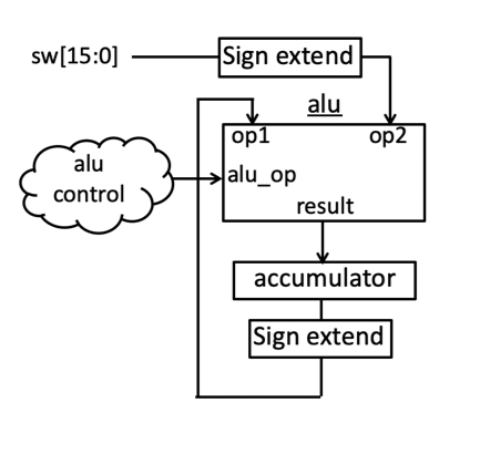
Create a 16-bit register (called the accumulator) to hold the contents of the current value of the calculator.
Use a always_ff@ block for this register.
Design your register as follows:
- The accumulator should be connected to the global clock input
- The accumulator should reset to zero using a synchronous reset when the ‘up’ button (btnu) is pressed
- The input to the accumulator should be the lower 16-bits of the 32-bit result output of the ALU
- The accumulator should be updated once every time the ‘down’ button (btnd) is pressed (use the one shot filter from the previous lab for this)
- Attach the value of the accumulator to the LED outputs
Connect the inputs to the ALU as follows:
- Create a 32-bit signal that is a sign extended version of the 16-bit accumulator. Attach this signal to the ‘op1’ input of the ALU
- Create a 32-bit signal that is a sign extend version of the 16-bit switch inputs. Attach this signal to the ‘op2’ input of the ALU
- Connect the lowest 16-bits of the ‘result’ output to the input of the accumulator (as discussed above)
- Create a new signal for the ‘alu_op’ signal and generate the logic for this signal as discussed below.
You can create a 32-bit sign extended signal using the Verilog ‘concatenation’ operator (i.e., concat the top bit of the signal you are sign extending and replicate it as many times as necessary). Search online about the ‘concatenation’ and ‘replication’ operator to review the syntax of these operators.
The ‘alu_op’ signal determines which ALU operation to perform. You will determine which operation to perform based on the value of the three buttons: btnl, btnc, and btnr. You do not need the ‘oneshot’ or ‘synchronizer’ for these three buttons since they will be read immediately when ‘btnd’ is pressed. You do need the ‘oneshot’ and ‘synchronizer’ for the ‘btnd’ buttons since these buttons control when the accumulator is updated.
Create a combinational circuit that generates the proper ‘alu_op’ signal based on the value of these three buttons as follows:
| Module Name: calc | ||||
|---|---|---|---|---|
| btnl | btnc | btnr | Function | alu_op |
| 0 | 0 | 0 | Add | 0010 |
| 0 | 0 | 1 | Sub | 0110 |
| 0 | 1 | 0 | AND | 0000 |
| 0 | 1 | 1 | OR | 0001 |
| 1 | 0 | 0 | XOR | 1101 |
| 1 | 0 | 1 | Less Than | 0111 |
| 1 | 1 | 0 | SLL | 1001 |
| 1 | 1 | 1 | SRA | 1010 |
If you use the constants defined in the riscv_alu_constants.sv file for your top-level design, you also need to include this file in your calc.sv file like you did for the alu.sv file.
You will need to create a combinational circuit that converts the three bit value specified by the three buttons to the corresponding four-bit alu_op value for the ALU. The following table demonstrates how this circuit should operate after setting the buttons and switches:
| btnl,btnc,btnr | Previous Value | Switches | Function | New Value after btnd |
|---|---|---|---|---|
| (Press btnu for reset) | xxxx | xxxx | Reset | 0x0 |
| 0,1,1 | 0x0 | 0x1234 | OR | 0x1234 |
| 0,1,0 | 0x1234 | 0x0ff0 | AND | 0x0230 |
| 0,0,0 | 0x0230 | 0x324f | Add | 0x347f |
| 0,0,1 | 0x347f | 0x2d31 | Sub | 0x074e |
| 1,0,0 | 0x074e | 0xffff | XOR | 0xf8b1 |
| 1,0,1 | 0xf8b1 | 0x7346 | Less Than | 0x0001 |
| 1,0,1 | 0x0001 | 0xffff | Less Than | 0x0000 |
Once you have created your calculator circuit, remove all syntax errors and open the simulator with your top-level circuit.
It may take some iterations in starting the simulator to identify and remove all errors.
Once your circuit is successfully in the simulation and all syntax errors have been removed, simulate your circuit by creating a custom simulation .tcl script.
Create TCL simulation file named calc_sim.tcl that performs the following simulation steps:
- Create an oscillating clock for the input clock
- Press btnu to issue a global reset
- Implement the operations shown in the table above
You will need to submit your simulation calc_sim.tcl file as part of your “Pass Off” below.
Exercise #4 - Calculator Testbench Simulation
In this exercise, you will simulate your calculator with another testbench file named tb_calc.sv that is included with your lab starter code.
Like the testbench used for the alu, this testbench instances your calculator module and provides a stimulus to the inputs and monitors the outputs.
When running the xvlog command to analyze your files you will need to add the flag --include ../include to specify the location of the riscv_alu_constants.sv file.
In addition, you will need to analyze the oneshot and synchronizer files from the previous lab since these modules are used in your calculator design.
Create a makefile rule named sim_tb_calc that runs the simulator with your calculator module and the testbench file.
This makefile rule should generate a file named sim_tb_calc.log.
Simulate your calculator circuit until you have removed all errors and successfully pass the testbench.
What is the final value of the accumulator at the end of the simulation?
Exercise #5 - Implementation and Download
In this final exercise, you will go through the steps required to synthesize, implement, and generate a bitstream for your ‘alu’ module. You will also download the module to the Basys3 board.
Synthesis
Create a .xdc file for your calc design and include it in your repository.
Create a makefile rule named calc_synth.dcp to run this synthesis script.
This rule should generate a synthesis logfile named calc_synth.log as well as the design checkpoint file calc_synth.dcp.
Run your makefile rule to generate the .dcp file and review the log file.
Implementation
After successfully synthesizing your design, create an implementation Tcl script to perform all the implementation steps.
When creating this script, you will need to add the option -include_dirs {../include} in your synth_design command to include the directory where your riscv_alu_constants.sv file is located.
synth_design -top calc -part xc7a35tcpg236-1 -verbose -include_dirs {../include}
Create a makefile rule named calc.bit to run this implementation script.
This makefile rule should generate the calc.bit bitfile as well as the following log and report files:
calc_imp.logcalc_utilization.rptcalc_timing.rpt
Test your makefile rule manually on the command line.
Indicate the number of resources consumed by this design and the timing (Worst Negative Slack) in the laboratory report.
Download
Once you have successfully generated a bitstream for your calculator circuit, download this bitstream to your Basys3 board. Experiment with your circuit and verify that it functions as expected. A TA will regenerate your bitstream from your submitted repository and validate that it works correctly.
Pass Off
The final step in the laboratory process is to complete the ‘pass off’. Carefully review the instructions for Git Submission as you prepare your submission for this lab. You will need to run the following command successfully to submit your lab:
python3 passoff.py --submit
Include the following information at the end of your laboratory report.
How many hours did you work on the lab?
Provide any suggestions for improving this lab in the future
How did you use AI to help you with this lab
-
You may wonder why four bits are needed to encode only nine operations. The four bits may specify up to 16 different operations. The RISC-V can perform a number of other operations that we will not implement in this course. To remain compatible with the description in the textbook we will stick with the four bits and the encoding described in the text. ↩