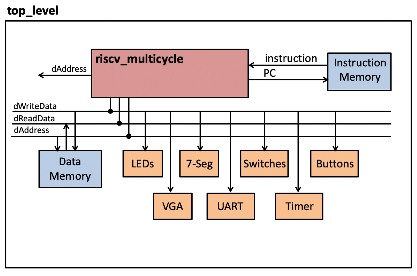
The RISC-V processor that you have developed over the semester will be inserted into a top-level design that includes other logic that will be provided for you. This logic will allow your processor to interact with a default memory configuration as well as the various input/output devices on the FPGA board such as the LEDs and switches. Your processor will be able to control and interact with these devices. A high-level overview of your processor system is shown below:
This page provides an overview of the system resources available within the given system project and a programming reference for the system. The base system includes the following resources:
- Instruction Memory
- Data Memory
- 5 Buttons
- 16 Switches
- 16 LEDs
- Seven Segment Display
- Timer
- UART
- VGA Display
Memory Organization
The system that has been created for you has several different address regions, each with a specific and important purpose. The purpose of these memory regions is summarized below:
| Address Range | Size (bytes) | Purpose |
|---|---|---|
| 0x00000000 - 0x00001fff | 8192 | Instruction Memory (.text) |
| 0x00002000 - 0x00003fff | 8192 | Data Memory (.data) |
| 0x00007f00 - 0x00007fff | 256 | Memory Mapped I/O |
| 0x00008000 - 0x0000bfff | 16384 | VGA Space |
Instruction Memory
The instruction is the region that contains the instructions of the program that is being executed. This memory is read only and cannot be changed during run-time. The instruction memory is fixed at 8192 bytes (or 2048 instruction words) and is mapped to adddresses 0x00000000 - 0x00001fff. All programs wil begin at address 0x00000000.
The program is initialized inside of the bitstream of your full system.
You can set the initial program that is compiled into your bitstream by setting the top-level TEXT_MEMORY_FILENAME generic before synthesizing and implementing your design.
The program loaded into this memory can be changed in the bitstream after implementation by running the load_mem.tcl script as described here.
Data Memory
This is the region that contains the global data memory. There are 8192 bytes or 2048 words. The top of this region is used for the stack and the bottom of this region is used for global data memory.
The data segment is initialized inside of the bitstream of your full system.
You can set the initial program that is compiled into your bitstream by setting the top-level DATA_MEMORY_FILENAME generic before synthesizing and implementing your design.
The data segment loaded into this memory can be changed in the bitstream after implementation by running the load_mem.tcl script as described here.
Memory Mapped I/O (mmio)
This region is allocated for specific I/O devices such as the LEDs. The I/O devices that have been added to this system can be controlled and monitored by writing data to and reading data from reserved memory locations that are dedicated to I/O devices in the system. This approach for controlling I/O is called “Memory Mapped I/O”. Memory Mapped I/O includes dedicated decoding logic within that monitors the address and control signals coming out of the RISC-V processor. When this decoding logic observes a write operation (caused by the ‘sw’ instruction) at the specific location of a I/O device, it intercepts this write and sends the data to the appropriate I/O device. The I/O devices act just like a memory in that they accept data from the ‘sw’ instruction and provide data back to the processor from the ‘lw’ instruction.
256 bytes of address space has been reserved for the I/O devices in this system. The I/O space is located at 0x0000_7f00 (i.e., 0x0000_7f00 - 0x0000_7fff). Each individual I/O device in this system has a specific address reserved within this range and is represented as an 8-bit offset. For example, the I/O device with an offset of 0x18 is located at 0x000_7f18. The I/O space reserved for the system you are using is summarized in the table below:
| I/O Offset | Read | Write |
|---|---|---|
| 0x00 (0) | Read value of LEDs | Write LED values |
| 0x04 (4) | Read Switch status | N/A |
| 0x08 (8) | TX Status | Write value to UART TX FIFO |
| 0x10 (16) | RX data | N/A |
| 0x14 (20) | RX status | N/A |
| 0x18 (24) | Seven Segment Display Value | Seven Segment Display Value |
| 0x24 (36) | Read Buttons status | N/A |
| 0x30 (48) | Timer (ms) | New Timer value |
| 0x34 (52) | Character Color | Character Color |
LEDs
Your RISC-V processor is able to control the 16 LEDs that are provided on the Basys 3 board. You can turn these LEDs on by writing data to address 0x0000_7f00 (0x0000_7f00 + 0). Writing to this memory location using a store word (‘sw’) instruction will set the value of the 16 LEDs. Bit 0 of the word corresponds to LED 0, bit 1 corresponds to LED 1, and so on. Note that since there are 16 LEDs and 32 bits in a word, the upper 16 bits written to this address location will be ignored. The bit value ‘1’ corresponds with turning ‘on’ the corresponding LED.
The following code example demonstrates how to write the value 0xa5 to the LED registers.
    # Assumes that x3 contains the I/O address space
    .eqv LED_OFFSET 0x0
    addi x6, x0, 0xa5
    sw x6, LED_OFFSET(x3)
This example will turn ON the following LEDs: LED7, LED5, LED2, and LED0. All other LEDs will be turned off.
Note that you can also read from this memory location using the load word (‘lw’) instruction to determine which LEDs are currently turned on (as dictated by a previous ‘sw’ instruction to the LEDs). The following example demonstrates how to read the values being displayed on the LEDs.
lw t0, LED_OFFSET(x3)
Switches
The memory mapped address 0x0000_7f04 (0x0000_7f00 + 0x04) corresponds to the slide switches. Reading from this memory location will indicate which switches are in the “on” (up) position. Bit 0 of the resulting word corresponds to the status of SW0 (right-most switch), bit 1 corresponds to SW1, and so on. Since there are only 16 switches, the top 16 bits of this word will always be zero. Writing a value to this memory location will not do anything. The following code example demonstrates how to read the switches:
    # Read the switches from 0x00007f04 by providing an offset of 4 to t0
    # (t0 + 4 = 0x00007f04)
    .eqv SWITCH_OFFSET 0x4
    lw t1, SWITCH_OFFSET(x3)
    # The value of the switches is now in t1
Buttons
The address 0x0000_7f24 (0x0000_7f00 + 0x24) corresponds to the push buttons. Reading from this memory location will indicate buttons which are pressed. When a button is pressed, the bit corresponding to the button will have the value ‘1’. The relationship between bit location and button is summarized in the table below:
| 4 | 3 | 2 | 1 | 0 |
|---|---|---|---|---|
| UP | RIGHT | DOWN | LEFT | CENTER |
| BTNU | BTNR | BTND | BTNL | BTNC |
The following example demonstrates how to read the buttons, branch back when the ‘down’ button (BTND) NOT pressed, and then fall through when the ‘down’ button IS pressed:
    # It is better to use constants when programming I/O
    .eqv BUTTON_OFFSET 0x24
    .eqv BUTTON_D_MASK 0x04
    # Assume x3 has the I/O base address
wait_for_btnd:
    # Read the buttons
    lw t1, BUTTON_OFFSET(x3)
    # Mask the buttons for button D
    andi t1, t1, BUTTON_D_MASK
    # If button d is not pressed, branch back
    beq t1, x0, wait_for_btnd:
button_d_pressed:
    # fall through after button d is pressed
Seven Segment Display
Address 0x0000_7f18 (0x0000_7f00 + 0x18) corresponds to the seven-segment display. Writing to this memory location will cause the lower 16-bits of the word being written to at this address to be displayed in hex on the four digits of the seven segment display. Like the LEDs, you can read the value of this memory location to see what value is currently being displayed on the seven-segment display. The following code segment demonstrates a loop that continuously updates the value of the seven segment display:
    .eqv SEVEN_SEGMENT_DISPLAY_OFFSET 0x18
    addi t1, x0, 0
loop:
    sw t1, SEVEN_SEGMENT_DISPLAY(x3)
    addi t1, t1, 1
    beq x0, x0, loop
Timer
A simple timer has been added to the system to provide a time stamp to facilitate timing accurate interactions. When the timer is read (0x0000_7f30), it will return the number of milliseconds since the processor was first turned on or since it was last reset. The timer can be loaded with any value by writing to the same address location (this is a convenient way to reset the timer). The following code example demonstrates how to wait for 10 ms:
    .eqv TIMER 0x30
    sw x0, TIMER(x3)      # Clear timer to zero
    addi t1, x0, 10       # Set t1 to 10 (10 milliseconds)
wait:
    lw t2, TIMER(x3)
    beq t2, t1, after_wait
    beq x0, x0, wait
after_wait:
UART
The circuit included with your processor also contains a “Universal Asynchronous Receiver/Transceiver” (UART). You should be familiar with a UART and what it does from the ECEN 220 course. This module will allow you to send bytes of data to a computer and receive bytes from the computer when typed in a terminal program. This will allow you to interact with your FPGA board from a computer terminal. You can send bytes over the UART and receive bytes from the computer by reading and writing to memory locations dedicated to the UART. The UART included with this system has a baudrate of 115200 and uses even parity.
To send a byte over the UART transmitter, first check to see if the transmitter is busy by reading the TX status register at address (0x0000_7f08). The first bit of this status register indicates whether the TX module is busy or not. If it is busy, wait until the status register indicates that the TX module is no longer busy - if you try to write a byte over TX while it is busy, the request will be ignored. Once the TX module is no longer busy, you can issue a transmission over the UART by writing to address 0x0000_7f08. Writing this register will cause the TX module to transmit the lower 8 bits of the word you write over the UART.
| Bits | Function |
|---|---|
| TX Status Register (read) - 0x0000_7f08 | |
| 0 | TX Busy |
| TX Control Register (write) - 0x0000_7f08 | |
|---|---|
| [7:0] | Write the 8 bit byte over the UART |
The following example demonstrates a transfer over UART:
    .eqv UART_TX 0x08
    .eqv UART_TX_BUSY 0x1
wait_for_tx_not_busy:
    lw t0, UART_TX(x3)
    andi t0, t0, UART_TX_BUSY
    bne x0, t0, wait_for_tx_not_busy
    # send word
    sw t1, UART_TX(x3)
To receive a byte from the UART receiver, first read the RX status register at address 0x0000_7f14 to see if there is a new byte available. If there is a new byte available, read the actual byte by reading the RX data register at address 0x0000_7f10. When this register is read, the “new byte” flag will be reset to zero. The RX status register has three flags indicating whether there is a new byte available, RX busy, and whether there was an error during the last RX transfer.
| Bit | Function |
|---|---|
| RX Status Register - read (0x0000_7f14) | |
| 0 | New data available from RX |
| 1 | The RX unit is busy |
| 2 | The previous RX transmission had an error |
| RX Data Register - read (0x0000_7f10) | |
|---|---|
| [7:0] | Read received data |
The following example demonstrates how to receive a word from the UART:
    .eqv UART_RX_STATUS 0x14
    .eqv UART_RX_DATA 0x10
    .eqv UART_RX_DATA_READY 0x1
wait_for_rx_data:
    lw t0, UART_RX_STATUS(x3)
    andi t0, t0, UART_RX_DATA_READY
    beq x0, t0, wait_for_rx_data
    # ge word
    lw t0, UART_RX_DATA(x3)
VGA
A VGA display controller is included in the I/O devices and can be programmed by the processor. This controller organizes the 640x480 display into a text character display that can display 80x30 characters (with each character having size 8x16). This controller allows you to place ASCII text characters on the screen at any of these 80x30 locations. Each character on the VGA screen is mapped to a different address location and control of the VGA display involves writing data to specific locations within this memory. The base location of the VGA display is 0x0000_8000 and the display consumes 16384 bytes (0x0000_8000 through 0x0000_bfff).
An ASCII character can be written to a specific location on the screen by writing the 8-bit ASCII value to the appropriate address. The address of each of the 80x30 character locations is determined by the following table:
| Base Address | Row Address | Column Address |
|---|---|---|
| addr[31:14] | addr[13:9] | addr[8:2] |
For example, the address of the location 24,13 (0x18,0xd) is 0x0000_8000 + 0xd << 9 + 0x18 << 2 = 0x0000_8000 + 0x1a00 + 0x60 = 0x0000_9A60. Writing the value 0x21 to this value will place the character “!” at the location (column,row) = 24,13 as shown in the following code:
    li t0, 0x00009A60
    addi t1, x0, 0x21
    sw t1, 0(t0)
Note: The li pseudo instruction involves the use of both the lui and the addi instruction.
We currently do not have the ability to execute the lui instruction so we will use other instruction sequences to do this for the lab.
The color of the characters on the VGA can also be controlled by the assembly instructions. All colors are specified by a “RGB” 12-bit value. The top four bits [11:8] specify the “Red” component of the color, bits [7:4] specify the “Green” component of the color, and the lower four bits [3:0] specify the “Blue” component of the color. The four bits associated with each primary color indicates the intensity of the given primary color. A value of “0000” for any of the primary colors will provide none of the given color while a value of “1111” for a primary color indicates provide this primary color at its maximum intensity. The table below demonstrates eight different colors that can be generated with this 12-bit color signal:
| Red [11:8] | Green [7:4] | Blue [3:0] | |
|---|---|---|---|
| 0000 | 0000 | 0000 | Black |
| 0000 | 0000 | 1111 | Blue |
| 0000 | 1111 | 0000 | Green |
| 0000 | 1111 | 1111 | Cyan |
| 1111 | 0000 | 0000 | Red |
| 1111 | 0000 | 1111 | Magenta |
| 1111 | 1111 | 0000 | Yellow |
| 1111 | 1111 | 1111 | White |
With 12 bits, you can create up to 4096 different colors. Each printed character appears on the display as two colors: the foreground (the color of the pixels that make up the character shape) and the background (the color where the character pixels do not exist). By default, all characters share the same foreground as background colors (this can be changed if necessary). The color of the foreground and background can be set by the VGA color register located at address 0x000_7f34. Bits [11:0] in this register determine the RGB color of the foreground and bits [23:12] determine the RGB color of the background as shown in the following table:
| Reserved | Background Color | Foreground Color |
|---|---|---|
| [31:24] | [23:12] | [11:0] |
| 00000000 | RRRRGGGGBBBB | RRRRGGGGBBBB |
In addition to setting a default foreground/background color, it is also possible to set a custom foreground and background color for each character on the display. This allows you to create interesting colored characters with differing backgrounds that move around on the display.
To set a custom foreground and background color for a particular location on the VGA display, write a value to the character location with a non-zero color set in the upper 25 bits of the 32-bit word. If any bits [31:8] are non-zero, the VGA memory will store the store bits [19:8] into the foreground color for the character and store bits [31:20] into the background color for the character. The 32-bits used by the VGA character memory are defined as follows:
| Background Color | Foreground Color | Unused | Character Value |
|---|---|---|---|
| data[31:20] | data[19:8] | data[7] | data[6:0] |
For example, to write the character “!” (ASCII 0x21) with a red foreground color (0xf00) and a blue background color (0x00f), you would write the following value to the VGA display:
0x21 | (0xf00 << 8) | (0x00f << 20) = 0x00ff0021
To write the character “$” (ASCII 0x24) to the display using the default background and foreground, then write the character value 0x24 to the memory (bit 7 is zero for 7-bit ASCII characters).