Table of Contents
Lab 11 - Final Processor
For this laboratory you will modify your pipelined processor from the previous lab to implement several new instructions and prepare your processor for download. You will also modify your Fibonacci code from a previous lab to execute on your processor.
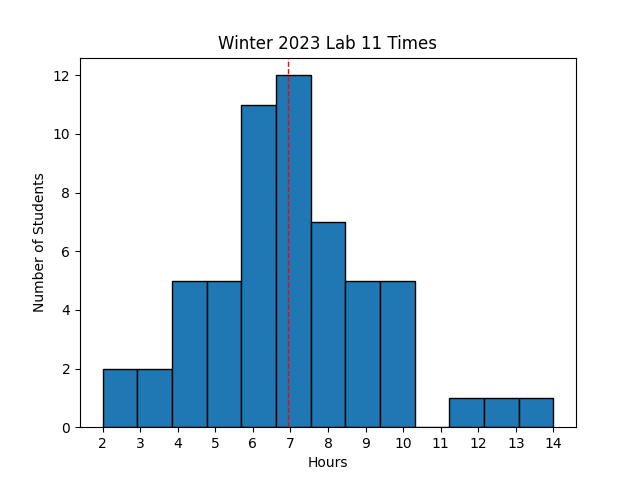 Avg Hours: 7.3, 7.3 (Winters 2022, 2021)
Learning Outcomes
- Understand how to implement jump instructions
- Modify the pipelined processor to implement several other instructions
Preliminary
In this laboratory exercise you will be adding a number of new instructions to your pipeline processor. Several preliminary exercises will be given to help you prepare for these processor changes. The instructions you will add include:
- Load upper-immediate Instruction: LUI
- Branch Instructions: BNE, BLT, BGE
- Jump Instructions: JAL, JALR,
The changes required to implement these instructions will be discussed below.
Load Upper Immediate Instruction, LUI
One of the limitations of the current processor is that we can only load immediate values that are 12-bits long (i.e., addi). This makes it difficult to create 32-bit constants and pointers to locations in memory that are far away from the current PC. To facilitate the creation of larger immediate values, you will need to implement the “load upper immediate” or LUI instruction. Review the operation of the LUI instruction by referring to the green card in your book or with the online RISC-V instruction set specification.
Determine the value written to the register x2 using the following LUI instruction (encoded): 0x03f2c137
There are several changes you will need to make to your processor to support this instruction. First, you will need to augment your “immediate generation” logic to generate a 32-bit immediate value using the “U-type” immediate format. In the ID stage you will need to decode the LUI instruction and when this instruction is found, generate the proper U-type immediate value.
The second change that should be made is to modify your control logic to support the unique functionality of the LUI instruction. The control logic should be modified so that the LUI instruction operates much like the ADDI (add immediate instruction). There is one key difference between the ADDI and the LUI: for the LUI, you should make sure that the register you read from the first read port (rs1) is always set to zero. The idea is that you want the new immediate value to be added to the value 0 (which is located in register 0). The result of the add will be the immediate value and this value can be written to the proper register in the register file as occurs with immediate instructions. Also, don’t forget that the RegWrite signal needs to be asserted for this instruction since it writes to the register file.
Branch Instructions
Your processor currently only supports one branch instruction: BEQ. You are required to add support for the following additional instructions: BNE (branch not equal), BLT (branch less than), and BGE (branch greater than or equal). Adding support for these instructions will require several changes to your processor. First, you will need to generate a “LESS_THAN” signal in the EX stage. This “LESS_THAN” signal indicates that the first operand of the ALU is “less than” the second operand of the ALU. This is easily obtained by evaluating the result of the subtract that occurs in the ALU during branch instructions. If the result is negative, then “LESS_THAN” should be true. Otherwise, “LESS_THAN” should be false. Like the “ZERO” signal, this signal needs to be pipelined from the EX stage to the MEM stage.
The second change is that you will need to keep track of which branch operation you are performing (‘funct3’ bits in the B=type instruction format) and send them through the pipeline to the MEM stage. In the MEM stage, you will need to use these ‘funct3’ bits as well as the ZERO and LESS_THAN flags to determine whether or not the branch is taken.
Complete the table below and determine whether the given branch is taken or not.
| Branch | ZERO | LESS_THAN | Taken? |
|---|---|---|---|
| BEQ | 0 | 0 | N |
| BEQ | 0 | 1 | |
| BEQ | 1 | 0 | |
| BNE | 0 | 0 | |
| BNE | 0 | 1 | |
| BNE | 1 | 0 | |
| BLT | 0 | 0 | |
| BLT | 0 | 1 | |
| BLT | 1 | 0 | |
| BGE | 0 | 0 | |
| BGE | 0 | 1 | |
| BGE | 1 | 0 |
Jump Instructions
For this final processor, you will need to add the two “jump” instructions: ‘jal’ and ‘jalr’. These jump instructions are essential for complex control flow and required when using subroutines in your program code. We will use these instructions in our final processor that we download on the FPGA in the next lab.
Determine which statements apply to each jump instruction in the lab report
Complete the table below by decoding each instruction and determining the Jump Target. Assume that the current value of the PC is 0xc00 and that register x4 contains the value 0x00041c00.
| Binary Instruction | Assembly Instruction | Jump Target |
|---|---|---|
| 0x0100016f | jal x2 16 | 0xc10 |
| 0x7f020167 | ||
| 0xff5ff16f |
Jumps are control flow instructions and operate very similar to branches in that they change the value of the PC. Unlike branch instructions, jumps are unconditional meaning that they always change the PC. Because jumps are unconditional and do not require the result of the ALU operation, it is possible to load the PC with the new value earlier in the pipeline (such as in the EX stage). To keep our processor simplier, however, we will design our jumps to update the PC in the MEM stage for consistency with branches.
The following changes will need to be made to your processor to implement these two jump instructions:
- Compute the proper jump target,
- Write PC+4 to a register, and
- Implement proper control flow pipeline flushing
Each of these functions will be described below.
Computing Jump Target
Just like the branch instructions, the jump instructions must compute a new address for the PC. This address is called the “PC Target”. The PC target for the two jump instructions are different from each other and the PC Target generated by branch instructions. Your processor will need to compute the following three different “PC Target” values: branches, JAL, and JALR. Each of these will be reviewed below.
Branch PC Target
You already have logic in place to compute the branch PC target from your previous processor. This was done by adding the PC value of the branch instruction with the immediate value within the EX stage. The result was pipelined to the MEM stage.
JAL PC Target
The PC target for the JAL instruction is computed in a manner similar to the target for the branch instructions. For this instruction, the PC target is computed by adding an immediate value found within the instruction to the PC of the current jump instruction. The immediate value used by the JAL instruction, however, is different than the immediate value used by the branch instructions. The JAL instruction uses the J-immediate format and you will need to create new logic for implementing this new immediate form.
JALR
The PC target for the JALR instruction is computed differently than branches and JAL. The PC target is computed by adding the contents of a register (rs1) with an immediate value. The JALR instruction uses the same immediate value as the arithmetic/immediate instructions. Unlike the other two approaches, the PC is not used in the computation of the PC target for the JALR instruction.
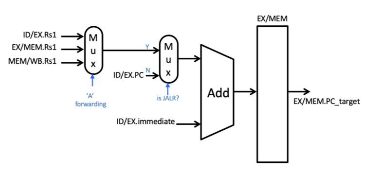
The following figure demonstrates how the dedicated adder used for computing the branch target in the EX stage can be modified to compute the PC target in the EX stage for all three situations. The key modification is the addition of a MUX that chooses between adding the PC (for the branch and JAL instructions) and the value of rs1 (for the JALR instruction). Note that since rs1 is used for the JALR instruction, forwarding logic is needed to forward values in the pipeline to this input.
Write PC+4 to a Register
The next capability that must be added to support the jump instructions is the ability to write the value of PC+4 into the register file. Like all instructions that write to the register file, the JAL and JALR instructions must write a value to the register file in the WB stage. As such, the RegWrite signal must be set high for both of these instructions when they are in the WB stage.
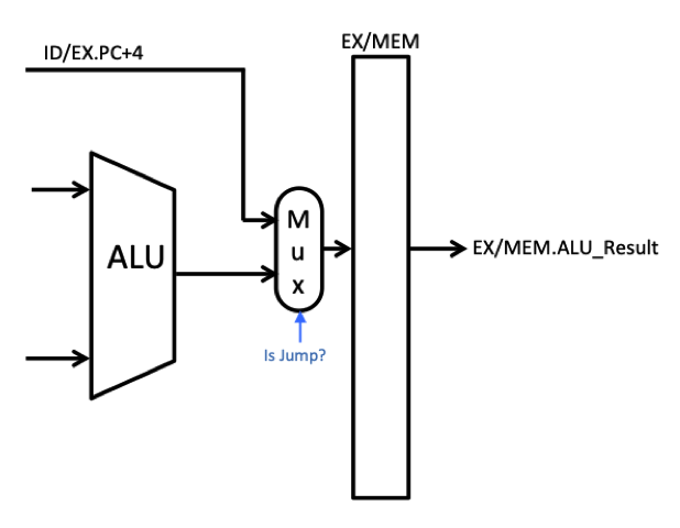
These two instructions must also compute the PC+4 value and make it available to the register file during the WB stage (i.e, written to the regWriteData port of the register file). There are a number of different ways of computing this value and passing it to the WB state. One relatively easy way to do this is to compute PC+4 in the EX stage and pass this value as the alu_result in the MEM stage. Once stored as the alu_result in the MEM stage, it will move down to the WB stage so that it can be written to the register file. The following modifications to your pipeline should be made (as shown in the figure below):
- Add an “+4” adder in the EX stage that computes ex_PC_plus_4 (i.e, ex_PC_plus_4 = ex_PC + 4)
- Add a multiplexer that selects between the output of the ALU and this ex_PC_plus_4 signal. For Jump instructions the multiplexer should select the ex_PC_plus_4. For all other instructions, the multiplexer should select the output of the ALU.
- The output of the multiplexer goes to the ALU_result pipeline register in the MEM stage (i.e., mem_alu_result)
Implement Pipeline Flushing
The last functionality needed to support jump instructions is to implement the control hazards. Because the jump instructions change the PC, it will cause control hazards. To simplify the changes needed to support jump instructions, we will address control hazards with jump instructions in the same way we do for branch instructions. Specifically, we will allow the jump instruction to proceed through the pipeline and then when it reaches the MEM stage, we will flush the three instructions behind the jump. Unlike branches, however, jumps are always taken and we will need to flush the pipeline each time a jump occurs. There are other more efficient ways to implement jumps, but we will stick with this approach to simplify the design. An example of the pipeline behavior for jumps is shown below. Note that you should make sure your jumps also handle the special ‘load-use-jump’ condition that was described for branches in the pipeline forwarding lab.
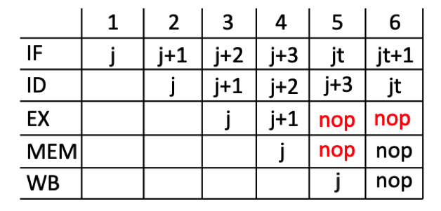
In the figure above, the ‘j’ represents either of the two jump instructions (‘jar’ or ‘jalr’). The ‘j+1’ instruction represents the instruction in the program memory immediately following the jump. The ‘jt’ instruction represents the jump target instruction.
- Place a NOP instruction in the EX and MEM stages in the clock cycle after the jump instruction is in the MEM stage.
- Place a NOP instruction in the EX stage in the clock cycle after the jump instruction is in the WB stage.
Exercises
Before proceeding with your laboratory exercises, update your repository with the latest lab starter code.
Exercise #1 - Support for Additional Instructions
The primary task of this lab is to modify your pipelined RISC-V processor from the forwarding lab to include support for additional instructions described in the preliminary. You should start this lab by copying your forwarding processor into a new file named “riscv_final.sv” and rename your top-level module to “riscv_final”. The parameter and ports for the final processor are the same as the previous lab.
| Module Name: riscv_final | |||
|---|---|---|---|
| Parameter | Width | Default Value | |
| INITIAL_PC | 32 | 0x00400000 |
| Port Name | Direction | Width | Function |
|---|---|---|---|
| clk | Input | 1 | Global clock |
| rst | Input | 1 | Asynchronous Reset |
| PC | Output | 32 | Program Counter in IF stage |
| iMemRead | Output | 1 | Enable instruction memory reading |
| instruction | Input | 32 | Current instruction in the ID stage |
| ALUResult | Output | 32 | Value of the ALUResult in the EX stage |
| dAddress | Output | 32 | Address for the data memory |
| dReadData | Input | 32 | Value of the data read from he MEM stage |
| dWriteData | Output | 32 | Value of the write data in the MEM stage |
| MemRead | Output | 1 | Data Memory Read signal |
| MemWrite | Output | 1 | Data Memory Write signal |
| WriteBackData | Output | 32 | Value of write data in the WB stage |
Once you have completed your logic changes to implement these instructions, synthesize your design to make sure there are no errors or important synthesis warnings.
Exercise #2 - Testbench Simulation
In this exercise you will simulate your final processor with a testbench and precompiled assembly language program.
The testbench will need to execute the program named final.s.
You will need to compile this assembly language program and generate a ‘text’ file, final_text.mem, and a ‘data’ file, final_data.mem (see the following tutorial for a review on how to assemble this file).
It will be very helpful to also generate a debug file, final_s.txt, that contains the assembled program and the original source.
The testbench is found in the lab starter code and is named riscv_final_tb.sv.
You will also need to add the ../include/tb_riscv.sv file by the testbench.
Also, add this ../include directory as an ‘include’ directory in your project.
The testbench contains a model of the RISC-V processor and the testbench will simulate your processor in parallel with the simulation model. The output provided by this testbench will provide a snapshot of the state of the simulation model at each clock cycle much like the previous two labs. If your processor differs from the simulation model then the testbench will exit with an error and give you a message explaining the problem. The testbench is designed to run until the “ebreak” instruction is executed. If your processor successfully reaches the “ebreak” instruction then you have passed the testbench (a “passed” message will be given).
Simulate this testbench and resolve all errors until your final processor is able to simulate without errors. The message you should get upon success is:
Passed! EBREAK/ECALL instruction reached WB stage at location 0x000001f4
Indicate the time at which the simulator stopped.
Exercise #3 - Fibonacci Sequence Code
Now that you have a complete processor that executes several of the instructions in the RISC-V instruction set, you are ready to write programs for your processor. For this exercise, you will modify an RISC-V assembly language program to compute the Fibonacci sequence using the subset of instructions supported by your processor. You will include two subroutines for computing the Fibonacci sequence - one that uses the iterative approach and one that uses the recursive approach. You will simulate this programs on the RARS simulator before simulating it Vivado operating on your RISC-V processor.
RARS Simulation
For this exercise, you will create two Fibonacci subroutines and insert them into a template assembly file named fib_template.s.
You should copy this file and rename it ‘fib.s’.
This program will call each of your Fibonacci sequence subroutines 15 times (each with an input of 0 to 14). The two Fibonacci subroutines you will create for this lab will be similar to those you completed in Lab #4 but with some important differences. These differences are as follows:
- Your new Fibonacci programs may only use the instructions that your RISC-V processor supports. You should not use any instruction that your processor cannot execute. Also, be careful when you use pseudo-instructions as these instructions may be replaced with instructions that may not be supported by your processor.
- You will only have one assembly language program rather than two (you will need to copy the subroutine portion only from each of your two files in lab 4 and insert them into the proper place of the template I gave you).
- In the RARS simulator, change the memory configuration to “Compact, Text at Address 0” (Settings->Memory Configuration, select “Compact, Text at Address 0”). This memory configuration organizes the segments as follows:
- .text: 0x00000000
- .data: 0x00002000
- stack pointer: 0x00003ffc
After adding your subroutines, simulate the program using the RARS simulator from Lab #4 to make sure your subroutines work properly.
You will need to include a copy of your modified Fibonacci code
What is the value of the ‘a0’ register when the program terminates with the ‘ebreak’ instruction?
How many instructions were executed to finish executing your program?
Testbench Simulation
Once your code operates properly within the RARS simulator, you are ready to simulate your program on your processor within Vivado. Before simulating your program, you need to generate the memory files used by the simulator. These memory files specify the contents of the instruction and data memory used by your processor. You can generate these files using the RARS assembler either with the GUI or on the command line. The instructions for generating these ASCII hexadecimal files is described in the tutorial used in the previous lab. You should have the following files after completing these steps:
- fib_text.mem
- fib_data.mem
After creating your memory files, create a new simulation ‘set’ using the create_fileset -simset sim_2 command (the first simulation set will simulate the final.s program from the previous exercise).
Include the following files in your new simulation set:
add_files -fileset sim_2 riscv_final_tb.sv  ../include/tb_riscv.sv
add_files -fileset sim_2 fib_text.mem fib_data.mem
Once you have created this new simulation set, set the simulation set as active.
Also, you need to set the the top-level parameters of the testbench to point to your new instruction and data simulation files.
The testbench has two parameters: ‘TEXT_MEMORY_FILENAME’ and ‘DATA_MEMORY_FILENAME’ that indicate which files to load for the instruction and data memories.
Set the properties of the testbench to point to these files in sim_2 with the following command:
set_property generic "TEXT_MEMORY_FILENAME=fib_text.mem DATA_MEMORY_FILENAME=fib_data.mem" [get_filesets sim_2]
After setting up your simulation with your new Fibonacci sequence, simulate your program until it terminates without an error. This program will take much longer to run than previous programs.
Indicate the time at which the simulator stopped in your Fibonacci code. Enter your number in nanoseconds. Every student’s stop time will be different, so any answer will receive full credit (your response will be used for statistical analysis.)
Exercise #4 - Synthesis
The final exercise in this lab is to synthesize your pipelined RISC-V processor. Carefully review your synthesis warnings to identify any potential problems with your processor that will prevent you from downloading it to the FPGA in the next lab.
Summarize the estimated resources for your synthesized logic in the table below.
| Resource | Estimation |
|---|---|
| LUT | |
| LUTRAM | |
| FF | |
| IO | |
| BUFG |
Pass Off
To create your submission, make sure the following files are committed in your ‘lab11’ directory:
- riscv_final.sv
- fib.s
Make sure you do not add unnecessary files (including Vivado project files) to your repository.
Test your submission by running the lab11_passoff.py pass-off script found in the starter code.
Review the instructions for submitting and passing off labs to make sure you have completed the lab properly.
How many hours did you work on the lab?
Provide any suggestions for improving this lab in the future