Table of Contents
Lab 10 - VGA Download
For this laboratory you will integrate the forwarding processor from the previous lab into the I/O sub-system and download your processor to the BASYS3 board. You will also learn how to use the VGA interface and change the program within your processor.
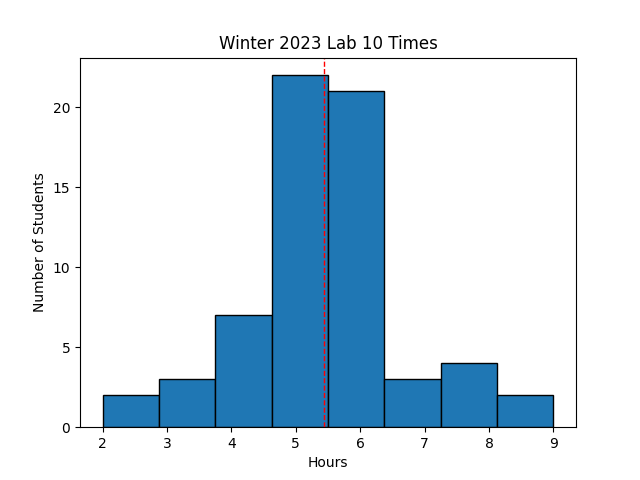 Avg Hours: 4.8, 4.2 (Winter 2022, 2021)
Learning Outcomes
- Learn how to program the VGA interface
- Learn how to create new programs for your processor system
Preliminary
Memory Mapped VGA
The logic added to your processor includes a display controller that can display text characters on a “VGA” display (VGA stands for “Video Graphics Adapter” and is an old display format that is not used much anymore). This VGA controller organizes the 640x480 display into a text character display that can display 80x30 characters (with each character having size 8x16). This controller allows you to place ASCII text characters on the screen at any of these 80x30 locations. Each character on the VGA screen is mapped to a different address location and control of the VGA display involves writing data to specific locations within this memory. The base location of the VGA display is 0x0000_8000 and the display consumes 16384 bytes (0x0000_8000 through 0x0000_bfff).
An ASCII character can be written to a specific location on the screen by writing the 8-bit ASCII value to the appropriate address. The address of each of the 80x30 character locations is determined by the following table:
| Base Address | Row Address | Column Address |
|---|---|---|
| addr[31:14] | addr[13:9] | addr[8:2] |
For example, the address of the location 24,13 (0x18,0xd) is 0x0000_8000 + 0xd << 9 + 0x18 << 2 = 0x0000_8000 + 0x1a00 + 0x60 = 0x0000_9A60. Writing the value 0x21 to this value will place the character “!” at the location (column,row) = 24,13 as shown in the following code:
    li t0, 0x00009A60
    addi t1, x0, 0x21
    sw t1, 0(t0)
Note: The li pseudo instruction involves the use of both the lui and the addi instruction.
We currently do not have the ability to execute the lui instruction so we will use other instruction sequences to do this for the lab.
Determine the address and ascii character value needed to place the character ‘$’ at column 38 and row 13 of the VGA display.
There are many online ASCII Tables you can use to find the proper ASCII code.
Determine the row, column, and character that is being written to the VGA by the following code sequence
    li t0, 0x0000a2fc
    addi t1, x0, 59
    sw t1, 0(t0)
The color of the characters on the VGA can also be controlled by the assembly instructions. All colors are specified by a “RGB” 12-bit value. The top four bits [11:8] specify the “Red” component of the color, bits [7:4] specify the “Green” component of the color, and the lower four bits [3:0] specify the “Blue” component of the color. The four bits associated with each primary color indicates the intensity of the given primary color. A value of “0000” for any of the primary colors will display none of the color while a value of “1111” for a primary color will display the color at its maximum intensity. The table below demonstrates eight different colors that can be generated with this 12-bit color signal:
| Red [11:8] | Green [7:4] | Blue [3:0] | |
|---|---|---|---|
| 0000 | 0000 | 0000 | Black |
| 0000 | 0000 | 1111 | Blue |
| 0000 | 1111 | 0000 | Green |
| 0000 | 1111 | 1111 | Cyan |
| 1111 | 0000 | 0000 | Red |
| 1111 | 0000 | 1111 | Magenta |
| 1111 | 1111 | 0000 | Yellow |
| 1111 | 1111 | 1111 | White |
With 12 bits, you can create up to 4096 different colors. Each printed character appears on the display as two colors: the foreground (the color of the pixels that make up the character shape) and the background (the color where the character pixels do not exist). By default, all characters share the same foreground as background colors (this can be changed if necessary). The color of the foreground and background can be set by the VGA color register located at address 0x000_7f34. Bits [11:0] in this register determine the RGB color of the foreground and bits [23:12] determine the RGB color of the background as shown in the following table:
| Reserved | Background Color | Foreground Color |
|---|---|---|
| [31:24] | [23:12] | [11:0] |
| 00000000 | RRRRGGGGBBBB | RRRRGGGGBBBB |
Determine the value to write to this register to set the foreground color as yellow and the background color as blue.
Exercises
Before proceeding with your laboratory exercises, update your repository with the latest lab starter code.
Exercise #1 - I/O Sub System for Forwarding Processor
In this first exercise you will simulate your processor from the previous lab executing within the I/O system executing a program that writes to the VGA. You will have a new top-level I/O design that you will insert your processor into. Begin this exercise by creating a new project for this lab by following these steps:
- Enter your ./lab10 directory and start vivado
- Enter the following command in the vivado tcl console to create a new project:
source create_forwarding_project.tcl
This script will integrate your forwarding processor from the previous lab with the I/O system you built in lab 7.
A simple test I/O program, forwarding_iosystem.s, has been written that operates on the I/O system described above.
Create the instruction memory file, data memory file, and debug file from this program by using the RARs assembler (the details of these command line options are described here):
java -jar ../resources/rars1_4.jar mc CompactTextAtZero a \
  dump .text HexText forwarding_iosystem_text.mem \
  dump .data HexText forwarding_iosystem_data.mem \
  dump .text SegmentWindow forwarding_iosystem_s.txt \
  forwarding_iosystem.s
This program has been compiled and is embedded in the instruction memory of the top-level system you were provided above. This program uses the buttons, switches, LEDs, and seven-segment display. Carefully review this program and answer the questions on Learning Suite about its functionality.
Answer the questions about the test program in Learning Suite
Add your ‘text’ and ‘data’ memory files associated with this project to your Vivado project.
add_files ./forwarding_iosystem_text.mem
add_files ./forwarding_iosystem_data.mem
set_property generic "TEXT_MEMORY_FILENAME=forwarding_iosystem_text.mem \
DATA_MEMORY_FILENAME=forwarding_iosystem_data.mem" [get_filesets sim_1]
You can simulate your processor operating with the top-level I/O system.
You can emulate the pressing of buttons and changing the switches by creating a .tcl script that changes these top-level inputs.
A template tcl file, vga_sim.tcl, has been created to help you get started with a TCL simulation.
When simulating this system with the precompiled program, you will receive messages indicating reads and writes to the I/O ports.
This script will run the processor for a long time to execute the clearing of the screen.
You should see many messages indicating data being written to the VGA display:
730000:Reading 0x00000000 from Switches
970000:Writing 0x00fff000 to Character Default Color
1120000:Writing 0x00000020 to VGA at address 0x00008000
1360000:Writing 0x00000020 to VGA at address 0x00008004
1600000:Writing 0x00000020 to VGA at address 0x00008008
1840000:Writing 0x00000020 to VGA at address 0x0000800c
2080000:Writing 0x00000020 to VGA at address 0x00008010
2320000:Writing 0x00000020 to VGA at address 0x00008014
2560000:Writing 0x00000020 to VGA at address 0x00008018
2800000:Writing 0x00000020 to VGA at address 0x0000801c
.
.
.
983690000:Writing 0x00000020 to VGA at address 0x0000bff8
983930000:Writing 0x00000020 to VGA at address 0x0000bffc
984200000:Writing 0x00000000 to Seven Segment Display
984230000:Writing 0x00000000 to LEDs
984290000:Reading 0x00000000 from Buttons
984470000:Reading 0x00000000 from Buttons
Copy this file into a new file named vga_sim_new.tcl and extend this tcl script to simulate the program writing to the VGA display with a character of your choosing.
Your script should do the following:
- Set the switches to the ‘!’ ASCII character (hex 0x21)
- Press the button-R
- Execute/run the simulation until the character is written on the screen.
Note: There is debouncing logic on the buttons that will require about 18 us before the button press is available from the I/O system.
You will need to simulate long enough for your button press to pass through this debouncing delay circuitry.
If your system is operating correctly, you should see a message in the log such as the following in which the value ‘0x21’ is written to the VGA address space (the time that this happens may not necessarily be the same as shown below):
1006900000:Writing 0x00000021 to VGA at address 0x00008004
You will need to include this .tcl file file as part of your lab submission
Exercise #2 - Download
After verifying your processor works correctly with the I/O system in simulation environment, you are ready to generate a bitstream of your system and download it to the Basys3 board. If your processor is designed correctly then it should be able to execute the sample test program that writes to the VGA display.
Your processor design has the instruction memory and data memory embedded within the FPGA. In order to generate your bitstream with the correct program, you will need to set several ‘synthesis’ properties within the Vivado tool. The Vivado TCL command below will (1) set the name of the file that contains the program to execute (i.e., the text segment), (2) set the name of the file that contains the initial data memory, and (3) set the debounce delay to 150 us (this is a longer debounce delay than the default debounce delay of 18 us).
set_property -name {STEPS.SYNTH_DESIGN.ARGS.MORE OPTIONS} -value { \
 -generic TEXT_MEMORY_FILENAME=forwarding_iosystem_text.mem \
 -generic DATA_MEMORY_FILENAME=forwarding_iosystem_data.mem \
 -generic DEBOUNCE_DELAY_US=150
} -objects [get_runs synth_1]
After setting these properties, generate the FPGA bitstream.
Summarize the utilized resources for your implemented design as well as the WNS.
| Resource | Estimation |
|---|---|
| LUT | |
| LUTRAM | |
| FF | |
| BRAM | |
| IO | |
| BUFG | |
| MMCM |
Once you have a bitstream, verify that the board and the VGA assembly language program operate on the VGA display as you expected. In order to test your design, you will need to connect your Basys3 board to a VGA monitor (see these instructions for details on how to do this on the lab computers). To demonstrate that your system is working properly, press the switches and buttons on the board such that you can write custom characters on the screen. Specifically, write your netID in the VGA display and take a picture of the display (with your phone or other camera). Name your file “vga.jpg” and try to limit the size of your file to a few megabytes.
You will need to include this image as part of your lab submission
Exercise #3 - Changing the Processor Program (Defuse)
For this exercise, you will be changing the program that is compiled into your FPGA bitstream. The steps involved in changing the program embedded in the bitstream are outlined in the following tutorial. You will be using this approach to upload your own programs to the bitstream in the future.
The program you need to insert into your bitstream is defuse.s.
This program simulates the defusing of a virtual “bomb”.
When first started, the VGA display is yellow indicating that the bomb is active.
You need to figure out what buttons and switches to set to defuse the bomb and turn the screen green.
If you make a mistake, the VGA display will turn red (i.e., explodes).
When you have defused the bomb, a code will be displayed on the display.
You can figure out what buttons and switches you must set by carefully reviewing the assembly code.
In this lab and future labs, you will be modifying the program frequently and it can be a hassle to download the bitstream using the Vivado Hardware Manager.
Another way for downloading the bitstream is to use the openocd command that has been installed on the digital lab computers (details about this command and how to use it can be found at the following link).
A python script has been created to simplify the process of downloading new bitstreams to the board.
The following python script will download the bitstream named defuse.bit to the FPGA board:
python3 ../resources/openocd.py defuse.bit
Note: This script will not work if the Xilinx Vivado environment has been set in your shell. If you are having problems running this script in a window in which the Vivado tool can be run, open a new fresh window without the vivado settings to run the script.
Enter the code displayed on the defused “green” screen when you have figured out how to defuse the circuit.
Exercise #4 - Custom Program
For the final exercise, you are to create your own custom assembly language program named move_char.s that operates as follows:
- On initialization of the program do the following:
- Clear the screen with the following color (red=0x9, green=0x2, and blue=0xe or 0x92e)
- Clear the value on the seven segment display
- Display your netid on screen starting at column 60 and row 24. Write your netid with a foreground color of 0xf80 and use the same background color as the cleared screen
- Display the ASCII character code 0x01 (a smiley face) at the top-left corner of the screen (using the same foreground and background as your netid)
- Provide the ability to ‘move’ the character using the buttons BTNR,BTNL,BTNU, or BTND to move the character right, left, up, and down.
- This is similar to the code in the
forwarding_iosystem.scode with the difference that you need to clear the previous location with a space (0x20) so that it appears that the character is moving from one space to another rather than leaving a trail - Make sure the character is bounded to a 10 x 10 region on the screen. If the user tries to move the character out of the top 10x10 character spaces then ignore the button press
- Increment the value on the seven segment display every time a valid button move occurs
- This is similar to the code in the
- When BTNC is pressed, start the program over (i.e., clear the screen and move the character to the first location)
This program will be very similar to the forwarding_iosystem.s assembly language program in the starter code.
Feel free to copy as much of this code as needed to implement this functionality.
Pass Off
To create your submission, make sure the following files are committed in your ‘lab10’ directory:
- vga_sim_new.tcl
- vga.jpg
- move_char.s
Make sure you do not add unnecessary files (including Vivado project files) to your repository.
Test your submission by running the lab10_passoff.py pass-off script found in the starter code.
Review the instructions for submitting and passing off labs to make sure you have completed the lab properly.
How many hours did you work on the lab?
Provide any suggestions for improving this lab in the future