Table of Contents
Lab 8 - RISC-V Pipelining
For this laboratory you will design a pipelined datapath and control for the RISC-V processor. This pipelined version of the processor will not implement hazard detection or forwarding.
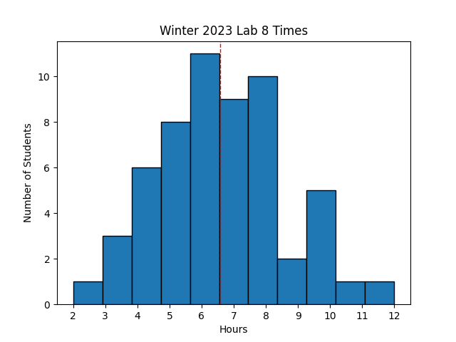 Avg Hours: 6.9, 6.1 (Winter 2022, 2021)
Learning Outcomes
- Learn how to create a pipelined version of your single-cycle RISC-V processor
- Understand the effects of instruction hazards and how to insert “NOP” instructions to prevent hazards
Preliminary
For this laboratory you are going to create a pipelined RISC-V processor. Pipelining is described in detail in Section 4.6 of the textbook and you may want to refer to the textbook as you complete this lab. You will also want to refer to the multi-cycle processor that you developed over the previous two labs. You will likely be copying and pasting portions of your processor code into this new lab.
As discussed in Sections 4.7 and 4.8 of the textbook, employing pipelining in the datapath of a processor introduces the notion of hazards. Hazards arise from data dependencies and control instructions. As described in the textbook, hazards can be handled by implementing forwarding and forcing stalls in your processor control logic.
To simplify the design of this pipelined processor, you will not need to implement any hazard checking, stalling, or forwarding (you will do this in the next lab). You will avoid hazards by inserting the appropriate number of “NOP” instructions in the assembly code (see page 322-323 of the textbook for a discussion of the NOP instruction). You will implement hazard detection and forwarding in the pipeline in the next lab. Because the use of “NOP” instructions are so important for preventing hazards in this lab, your processor needs to implement a “NOP”. A “NOP” is an instruction that does not activate any of the control signals that change the processor state. Although there is no “NOP” instruction, the assembler interprets the “NOP” pseudo instruction and replaces it with the instruction “addi x0, x0, 0” (0x00000013). When you execute this instruction there should be no changes in the processor register state.
For each of the following assembly language code sequences, determine the minimum number of NOP instructions that must be inserted before each instruction such that no hazards occur within a pipelined processor that does not implement forwarding.
Example #1
1: sub x2,x1,x3
2: and x12,x2,x5
3: or x13,x6,x2
4: add x14,x12,x2
5: sw x14,100(x13)
Example #2
1: ld x2, 20(x1)
2: and x4,x2,x5
3: or x8,x2,x6
4: and x9,x4,x2
5: sub x1,x6,x7
Example #3
For this example, assume that the branches occur in the MEM cycle as shown in Figure 4.48 (p. 310).
Include the number of NOPs for both control and data hazards.
1: beq x1, x0, 16
2: and x12,x2,x5
3: or x13, x6, x12
4: add x14,x12,x2
5: ld x4,100(x13)
Exercises
Before proceeding with your laboratory exercises, update your repository with the latest lab starter code.
Exercise #1 - Pipeline Datapath and Control
The pipeline that you will implement in this lab is shown in Figure 4.53 (p. 314) of the textbook. Review this figure carefully as you complete this lab. There are five stages of the pipeline: Instruction Fetch (IF), Instruction Decode (ID), Execute (EX), Memory Access (MEM), and Write-Back (WB). You will create logic for each of these stages in your pipelined processor. Note that you will not be reusing your code from labs 5 & 6 to complete this lab. You will likely need to refer to these files but you will need to start over with a fresh file for this lab.
Begin this exercise by creating the module interface and top-level ports as shown in the table below:
| Module Name: riscv_basic_pipeline | |||
|---|---|---|---|
| Parameter | Width | Default Value | |
| INITIAL_PC | 32 | 0x00400000 |
| Port Name | Direction | Width | Function |
|---|---|---|---|
| clk | Input | 1 | Global clock |
| rst | Input | 1 | Synchronous Reset |
| PC | Output | 32 | Program Counter in IF stage |
| instruction | Input | 32 | Instruction received from instruction memory |
| ALUResult | Output | 32 | Output of (EX stage) |
| dAddress | Output | 32 | Value of the data address in the MEM stage |
| dWriteData | Output | 32 | Value of the write data in the MEM stage |
| dReadData | Input | 32 | Value of the read data in the WB stage |
| MemRead | Output | 1 | Data Memory Read signal |
| MemWrite | Output | 1 | Data Memory Write signal |
| WriteBackData | Output | 32 | Data to be written to register (WB stage) |
After creating your top-level ports, create each of the five pipeline stages. Guidelines for logic required in each of these stages are discussed below. Create the entire pipeline in a single System Verilog module and dedicate different sections of your SystemVerilog code to each pipeline stage.
The logic you create in this module will be similar to the logic you created in the datapath and multi-cycle control labs. However, you will be creating this logic over again for this lab to take into account the pipeline registers. You should refer to the logic in these previous labs as you complete this pipelined processor. You will be reusing your ALU and register file from the previous labs.
Each pipeline stage will include the logic needed to implement the functionality of the stage as well as the pipeline registers to transfer data from one stage to the next. Guidelines for creating the logic and pipeline registers at each of the pipeline stages are described below. Make sure that all pipeline registers you create are reset to zero when the synchronous ‘rst’ is asserted.
NOTE: Coding Guidelines Creating a working pipeline RISC-V processor is a challenging task and the process is made difficult by using poor coding practices and styles. You should follow the following additional coding guidelines for the lab to help you more easily complete the lab. You will be penalized if you do not follow these lab-specific coding guidelines.
#1: Comments: Organize the logic for each pipeline stage in its own section in the code and provide a very clear comment on where the logic for the stage resides. This example below demonstrates an easy to find comment indicating the start of the ‘IF’ logic:
//////////////////////////////////////////////////////////////////////
// IF: Instruction Fetch
//////////////////////////////////////////////////////////////////////
#2: Signal Names: Pipelining is tricky in part because the same signal exists in multiple pipeline stages (i.e., PC in ID and IF stages).
To keep these signals straight, you should name them using the pipeline stage prefix. For example, the PC in the IF stage should be named “if_PC” and the PC in the ID stage should be named ‘id_PC’.
This way, you can easily identify the signal and the pipeline stage it belongs to.
Use the following text prefixes for each stage; ‘if’, ‘id’, ‘ex’, ‘mem’, and ‘wb’.
The pipelining figures in the textbook provide insight into the naming of signals.
For example, signals in the stage to the left of the “IF/ID” register should be given the ‘if’ prefix and signals to the right of the “IF/ID” register should be given the ‘id’ prefix.
Include Files: You will want to include the files riscv_alu_constants.sv and riscv_datapath_constants.sv which will contain constants used in your processor.
You may want to add new constants to these files as needed.
If needed, here is a review on how to use include files with constants in System Verilog.
Instruction Fetch (IF)
The IF stage manages the reading of the instruction memory and updating the program counter. The primary component of the IF stage is the Program Counter (PC). Begin your IF stage by creating the program counter (use the ‘if_’ prefix for the “IF” version of your PC). The program counter is used to address the instruction memory and needs to be updated every clock cycle. The PC should be set to the constant ‘INITIAL_PC’ when the synchronous reset is asserted.
The ‘PCSrc’ signal, generated in the MEM stage, determines what is loaded in the PC: PC+4 when ‘PCSrc’=0 and the branch target (computed in the MEM stage) ‘PCSrc’=1. The ‘PCSrc’ signal is set in the MEM stage (being generated in the MEM stage, it should be named ‘mem_PCSrc’). Unlike the previous multi-cycle processor lab in which an instruction is executed every five clock cycles, the PC should be updated every clock cycle in this pipeline since a new instruction is loaded every clock cycle.
The diagrams in the book include the instruction memory in the IF stage. You will not need to include the instruction memory in your IF state for this lab. In this lab the instruction memory will be placed in the testbench. The instruction memory used in the testbench will be a synchronous memory meaning that the output of the memory will appear one clock cycle after the address is presented. This means that the ‘instruction’ input to your processor is valid during the ID stage (i.e., you do not need to create a pipeline register for it - it is already pipelined).
The only information that you need to pipeline from the IF stage for the ID stage is the PC. Create the pipeline register for the PC and provide a unique name for the PC used in the ID stage by using the ‘id_’ prefix. For example, you should create the signal named ‘if_PC’ to represent the PC in the IF stage and a signal named ‘id_PC’ to represent the PC in the ID stage. This pipelined signal should also be initialized to ‘INITIAL_PC’ upon reset (as well as the ‘ex_PC’ signal that is pipelined from the ID stage to the EX stage).
Instruction Decode (ID)
The ID stage has several important functions including (1) decode the instruction and generate the control signals needed by subsequent stages, (2) generate the appropriate immediate values for use by the EX stage, and (3) read the registers from the register file. Each of these purposes will be described in more detail below.
1. Decode Instruction
An important function of the ID stage is to decode the instruction and generate the various control signals used by the subsequent pipeline stages. This decoding logic will take the ‘instruction’ input received from the instruction memory and generate each of the necessary control signals. The following control signals must be determined in the ID stage and pipelined for use in a later pipeline stage:
| Control Signal | Stage Used |
|---|---|
| ALUCtrl | EX |
| ALUSrc | EX |
| MemWrite | MEM |
| MemRead | MEM |
| Branch | MEM |
| RegWrite | WB |
| MemtoReg | WB |
Note that Figures 4.48 (p. 310) and 4.53 (p. 314) show that the funct3 bits ([14-12]) and one bit from funct7 ([30]) are passed from the ID stage into the EX stage and the ALUCtrl signal is generated in the EX stage. It doesn’t really matter whether you create the ALUCtrl signal in the EX stage as shown in the textbook or generated directly in the ID stage as suggested here.
Create the appropriate logic for each of these control signals and create pipeline registers to pass these control signals from the ID stage to the EX stage. Each of these signals should be set to zero when the synchronous reset is applied.
2. Immediate Generation
The ID stage must also generate the immediate value used within the EX stage. Create the logic for the immediate value and generate a pipeline register for this signal for the EX stage.
3. Register File
You will need to instance your register file from your previous lab to be used in the ID stage. The register accesses (i.e., register reads) are associated with the instruction in the ID stage. The read addresses for both read ports of the register file should be determined directly by decoding the current instruction in the ID stage.
Register writes are associated with the instruction in the WB stage. The instruction in the WB stage determines the ‘RegWrite’ signal, the write register address, and the value to be written to the register file. You will need to decode the write register address and the ‘RegWrite’ signal of the instruction in the ID stage and pipeline these signals to the WB stage. The pipelined versions of these signals in the WB stage should be hooked up to the register file The value to be written to the register file will be determined by the EX stage and pipelined to the WB stage.
Since the outputs of the register file are already registers you do not need to create pipelining registers for the outputs of the register file. These register file outputs will be valid for the EX stage and can be named accordingly (i.e., something like ‘ex_read1’).
You need to pipeline the value of the register write address since the register write operation associated with this instruction does not occur until the WB stage.
In addition to pipelining all of the signals generated in the ID stage, you must pipeline the PC signal in the ID stage for use in the EX stage.
Execute (EX)
The EX stage is responsible for (1) performing ALU operations and (2) computing the branch target address. Each of these functions will be described below.
1. ALU Operations
The primary funciton of the EX stage is to perform ALU operations. Instance the ALU from your previous lab and connect your ALU as shown in Figure 4.48 (p. 310). The input to the first ALU operand should be the output of the first register file read port (the read operation in the register file is already pipelined and thus valid in the EX stage). A multiplexer is needed to select the value of the second ALU operand. The pipelined ‘ALUSrc’ signal is used to determine whether the second register output or the immediate data is used for the second operand of the ALU. The pipelined ‘ALUCtrl’ control signal should be used to determine which operation to perform.
The output of the ALU must be pipelined for use in the following MEM stage. In addition, the ‘Zero’ signal must be generated from the ALU result and pipelined for use in the MEM stage as well.
2. Branch Target Address
The EX stage must also compute the branch target address. This is done by simply adding the pipelined ‘PC’ signal in the EX stage with the pipelined immediate branch offset. This computed branch target address must be pipelined for use in the MEM stage.
You must also create pipeline registers for control signals generated in the ID stage, passed to the EX stage, and used in a later stage of the pipeline. These signals include: ‘Branch’, ‘MemWrite’, ‘MemRead’, ‘MemtoReg’, ‘RegWrite’ as well as the register write address. In addition, you need to create a pipeline register for the read data 2 output from the register file for use as the write data in the MEM stage.
Memory Access (MEM)
The primary function of the MEM cycle is to perform memory accesses (for loads or stores). In addition, the decision on whether a branch is taken or not taken is made during this stage.
Data Memory
Like the Instruction Memory, the Data Memory is not included in your pipelined processor. Instead, you will need to provide the appropriate signals for an external data memory that will be provided in the testbench.
The address used for the memory comes from the ALU in the EX stage through a pipeline register. The data to write also comes from the EX stage through a pipeline register (from Read data 2). The control signals for MemWrite and MemRead were generated back in the ID stage and propagate through pipeline registers to the MEM stage.
Note: The data memory is pipelined meaning that reads occuring in the MEM stage will produce their result in the WB stage (like the pipelining of the register file). You do not need to pipeline the memory read to the WB stage since it is already pipelined internally.
Branch Logic
The MEM stage generates the control signal ‘PCSrc’ by ‘and’ing the ‘Zero’ signal with the ‘Branch’ signal. This signal is used in the IF stage to select between incrementing the PC and branching.
In addition to the branch logic, the following signals need to be pipelined for use by the WB stage: ‘ALU Result’, ‘MemtoReg’, ‘RegWrite’, and the register write address.
Write-Back (WB)
The final stage is the Write-Back (WB) stage whose purpose is to write-back results into the register file. The logic for this stage is relatively simple and involves a multiplexer that selects the data to be written: the ALU result or the memory read based on the pipelined ‘MemtoReg’ control signal.
Since this is the last pipeline stage there is no need to further pipeline any of the control signals.
Top-Level Ports
The last step of your pipelined processor is to drive the top-level ports. Some of these top-level ports are used by the testbench to watch the operation of your pipeline and verify its proper operation. You should have already created all of these signals within your pipeline but you will need to add ‘assign’ statements to assign the value of these top-level ports to their actual name within your pipeline.
The top-level ports that you need to drive are the following:
| Port Name | Signal within your pipeline |
|---|---|
| PC | Program Counter in IF stage |
| ALUResult | Value of the ALUResult in the EX stage |
| dWriteData | Value of the write data in the MEM stage |
| WriteBackData | Value of write data in the WB stage |
Exercise #2 - Testbench
For this exercise you will need to simulate your pipeline with the following testbench. This testbench contains the instruction and data memory and a simulation model of the RISC-V processor that is used to compare against your processor. You will need the following files for the testbench (found in the starter code):
| File | Purpose |
|---|---|
riscv_pipeline_tb.sv |
Top-level testbench file |
pipeline_nop.s |
The original assembly language file |
You will need to assemble the pipeline code to generate the instruction and data memory files needed by the simulator. The following command demonstrates how to generate these files:
java -jar ../resources/rars1_4.jar mc CompactTextAtZero a \
  dump .text HexText pipeline_nop_text.mem \
  dump .data HexText pipeline_nop_data.mem pipeline_nop.s
Once you have created these memory files you will need to add them to your project so you can simulate the execution of this program. It is often helpful to generate a debug text file that includes both the assembly as well as the binary instructions. The following command demonstrates how to generate such a debug file:
java -jar ../resources/rars1_4.jar mc CompactTextAtZero a \
  dump .text SegmentWindow pipeline_nop_s.txt pipeline_nop.s
You may want to refer to the assembly language file and this debug file as you debug your pipelined processor in the testbench.
Note that you will get the following warning in your simulation that you can safely ignore:
WARNING: Too many words specified in data file pipeline_nop_data.mem
Answer the questions about the debug file in learning suite.
When you have setup your simulation environment properly, you should see the following header lines on your TCL console indicating that the memory files and simulation environment are properly setup:
===== RISC-V Pipeline Simulation Model Version 1.2 =====
**** RISC_V Simulation model: Loaded instruction memory 'pipeline_nop_text.txt' ****
**** RISC-V Simulation model: Loaded data memory 'pipeline_nop_data.txt' ****
**** Testbench: Loaded instruction memory ****
**** Testbench: Loaded data memory ****
===== RISCV PIPELINE TESTBENCH V1.20 =====
 use run -all
The testbench provides a lot of information to help you debug your processor. During each cycle of operation the testbench will summarize what it thinks is in each pipeline stage and will highlight any errors in the pipeline. The following text demonstrates sample output from the testbench while your pipelined processor is being executed:
190 ns:No Errors
  IF: PC=0x00000040
  ID: PC=0x0000003c I=0x00000013 [nop]
  EX: PC=0x00000038 I=0x00000013 [nop] alu result=0x00000000
  MEM:PC=0x00000034 I=0x02100c63 [beq x0,x1,0x38] No memory read/write
  WB: PC=0x00000030 I=0x05a14413 [xori x8,x2,0x5a] WriteBackData=0xffffffa5
200 ns:No Errors
  IF: PC=0x00000044
  ID: PC=0x00000040 I=0x00000013 [nop]
  EX: PC=0x0000003c I=0x00000013 [nop] alu result=0x00000000
  MEM:PC=0x00000038 I=0x00000013 [nop] No memory read/write
  WB: PC=0x00000034 I=0x02100c63 [beq x0,x1,0x38] WriteBackData=0xfffff000
Continue debugging your pipeline until you are able to successfully pass the testbench. The message you should receive if you pass your testbench is as follows:
You Passed!
Indicate the time in which your testbench finished execution
Exercise #3 - Synthesis
The final exercise in this lab is to synthesize your pipelined RISC-V processor. Complete the synthesis process and carefully review the synthesis messages for unusual warnings.
Summarize the estimated resources for your synthesized logic in the table below.
| Resource | Estimation |
|---|---|
| LUT | |
| LUTRAM | |
| FF | |
| BRAM | |
| IO | |
| BUFG | |
| MMCM |
Note: The number of I/O that you use will exceed the capacity of the device. This is ok for this lab.
Pass Off
To create your submission, make sure the following files are committed in your ‘lab08’ directory:
- riscv_basic_pipeline.sv
Make sure you do not add unnecessary files (including Vivado project files) to your repository.
Test your submission by running the lab08_passoff.py pass-off script found in the starter code.
Review the instructions for submitting and passing off labs to make sure you have completed the lab properly.
Include the following information at the end of your laboratory report.
How many hours did you work on the lab?
Provide any suggestions for improving this lab in the future