Table of Contents
Lab 6 - RISC-V Control
For this laboratory you will design the control unit for a simplified, multi-cycle, non-pipelined datapath you designed in the previous laboratory. Your simple RISC-V processor will be able to execute simple assembly language programs.
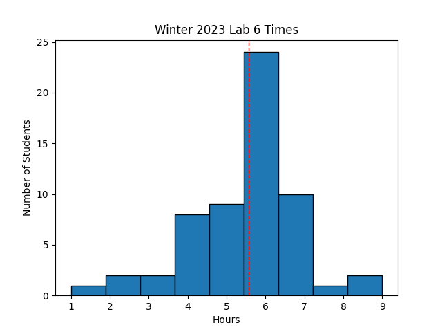 Avg Hours: 6.4, 5.6 (Winter 2022, Winter 2021)
Learning Outcomes
- Implement a multi-cycle control unit for the RISC-V datapath in SystemVerilog
- Verify the control unit of the RISC-V processor by executing a simple program
Preliminary
A simple single-cycle control implementation of the RISC-V processor is described in detail in Sections 4.4 (pages 269-283) of the textbook. You will need to understand this section of the book in great detail to complete this lab. You will likely need to refer to these sections of the textbook as you complete this lab. Make sure you have access to your textbook while completing this lab. You will be creating a controller for your datapath to implement the following 21 instructions:
| Type | Instruction |
|---|---|
| Arithmetic/Logic | add, sub, slt, sll, srl, sra |
| Arithmetic/Logic Immediate | addi, slti, slli, srli, srai |
| Logical | and, or, xor |
| Logical Immediate | andi, ori, xori |
| Branch | beq |
| Memory | lw, sw |
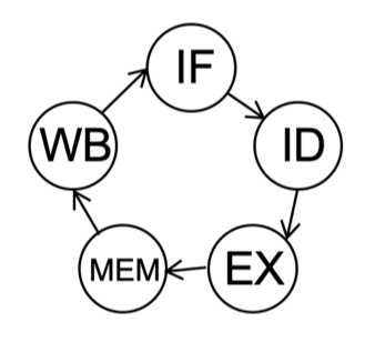
For this lab, you will be creating a multi-cycle controller that executes each instruction in five clock cycles. You will implement a state machine that sequences between the following five states for instruction execution:
| State | Purpose |
|---|---|
| IF | Instruction fetch: provide the PC to the instruction memory |
| ID | Instruction Decode: decode the received instruction and start register access |
| EX | Execute: execute the operation in the ALU |
| MEM | Memory: perform memory access (for ld/sd) |
| WB | Write Back: write new data into register file |
A state diagram demonstrating these instruction steps is shown below:
The primary purpose of this lab is to implement the state machine and generate the control signals for the datapath unit. The following discussion and set of questions will help you understand the logic you need to create the control signals.
ALUCtrl
‘ALUCtrl’ is a four-bit control signal that dictates the operation of the ALU. As described in the book and in the class lecture, generating the ‘ALUCtrl’ signal requires multi-level decoding involving the ‘opcode’ field of an instruction as well as the ‘funct3’ and ‘funct7’ bits. The decoding logic should set the ALU operation based on the instruction as follows:
- load and store: addition
- branch: subtraction
- ALU operations: operation based on funct3 and funct7 (including shift instructions)
To test your understanding of the decoding necessary for this signal, determine the value of the ALUCtrl signal for each of the following instructions:
| 32-bit instruction | ALUCtrl |
|---|---|
| 0x004b2283 | 0010 |
| 0x403100b3 | |
| 0x0ff0c193 | |
| 0x04510463 | |
| 0x01830493 | |
| 0x0078e533 | |
| 0x0062a233 | |
| 0x0028a623 | |
| 0x01d3f2b3 | |
| 0x00350533 | |
| 0x0163f293 | |
| 0x0ff9a693 |
ALUCSrc
When ‘ALUSrc’== 0, the register read 2 output is used as the input to operand 2 of the ALU. When ‘ALUSrc’== 1, immediate data for the input to operand 2 of the ALU (see Figure 4.19 in the text). Immediate data is needed for ‘load’, ‘store’, and ‘ALU Immediate’ instructions. You can determine the value of ‘ALUSrc’ directly from the opcode bits of the instruction.
Determine the value of the ‘ALUSrc’ signal for each of the following instructions (for instructions in which it doesn’t matter, enter a ‘0’ or a ‘1’).
| 32-bit instruction | ALUSrc |
|---|---|
| 0x004b2283 | 1 |
| 0x403100b3 | |
| 0x0ff0c193 | |
| 0x04510463 | |
| 0x01830493 | |
| 0x0078e533 | |
| 0x0062a233 | |
| 0x0028a623 | |
| 0x01d3f2b3 | |
| 0x00350533 | |
| 0x0163f293 | |
| 0x0ff9a693 |
MemRead and MemWrite
Two signals control the memory interface: ‘MemRead’ and ‘MemWrite’. The ‘MemRead’ signal is set for ‘load’ instructions and the ‘MemWrite’ signal is set for ‘store’ instructions. Unlike the previous signals, these signals should only be set during the ‘MEM’ stage of the instruction state machine.
Determine which of the following instructions should set the ‘MemRead’ signal and ‘MemWrite’ signals during the ‘MEM’ instruction stage:
(0x004b2283, 0x403100b3, 0x0ff0c193, 0x04510463, 0x01830493, 0x0078e533, 0x0062a233, 0x0028a623, 0x01d3f2b3, 0x01d3f2b3, 0x00350533).
MemtoReg and RegWrite
The ‘RegWrite’ signal is used to control when values are written to the register file. For this five-cycle execution sequence, ‘RegWrite’ should only be set to ‘1’ during the ‘WB’ state of the instruction state machine. Some instructions do not write back to the register file so this signal will stay low for the entire five clock cycle instruction sequence.
The ‘MemtoReg’ signal is based on the current instruction and is set to ‘1’ only when executing a ‘load’ instruction. This signal does not depend on the current state (it doesn’t matter what this signal is during all state except the ‘WB’ state).
Determine which instructions should set the ‘RegWrite’ signals during the ‘WB’ instruction stage.
loadPC and PCSrc
The ‘loadPC’ signal is used to update the PC with a new value. The ‘loadPC’ signal should be set to ‘1’ during the ‘WriteBack’ state of every instruction (thus loading a new PC value before entering the next IF state).
The ‘PCSrc’ signal is used to indicate which value to load to the PC: ether PC+4 for regular instructions or PC+branch_offset for branch taken operations. This signal is based on both the current instruction and on the value of the ‘Zero’ signal. This signal should be set to ‘1’ when the following conditions are present: (1) current instruction is a “BEQ” function, and (2) the Zero flag is high.
Assuming the Zero flag is high, determine which of the following instructions should set the ‘PCSrc’ signal to ‘1’.
Exercises
Before proceeding with your laboratory exercises, update your repository with the latest lab starter code.
Exercise #1 - Verilog RISC-V Processor
For this exercise you will implement the basic RISC-V processor as described in the textbook.
Begin your exercise by creating an empty Verilog module named riscv_multicycle.sv with the following top-level ports.
| Module Name: riscv_multicycle | |||
|---|---|---|---|
| Parameter | Width | Default Value | |
| INITIAL_PC | 32 | 0x00400000 |
| Port Name | Direction | Width | Function |
|---|---|---|---|
| clk | Input | 1 | Global clock |
| rst | Input | 1 | Synchronous Reset |
| instruction | Input | 32 | Instruction data from Instruction Memory |
| dReadData | Input | 32 | Data read from data memory |
| PC | Output | 32 | Program Counter |
| dAddress | Output | 32 | Address for data Memory |
| dWriteData | Output | 32 | Data to write into data memory |
| MemRead | Output | 1 | Control signal indicating memory read |
| MemWrite | Output | 1 | Control signal indicating memory write |
| WriteBackData | Output | 32 | Data being written to registers (for debug) |
Like the datapath module in the previous lab, your module should have a parameter for the INITIAL_PC. The following steps will guide you through the process of creating this module.
1. Datapath
The first step is to instance the datapath circuit you created in the previous lab. When you instance your datapath circuit, you should pass the INITIAL_PC parameter of this module to your datapath module. This parameter indicates the initial value in memory where your ‘.text’ segment will execute. The organization of the datapath circuit in relation to the control logic and the top-level ports is shown in the figure below:
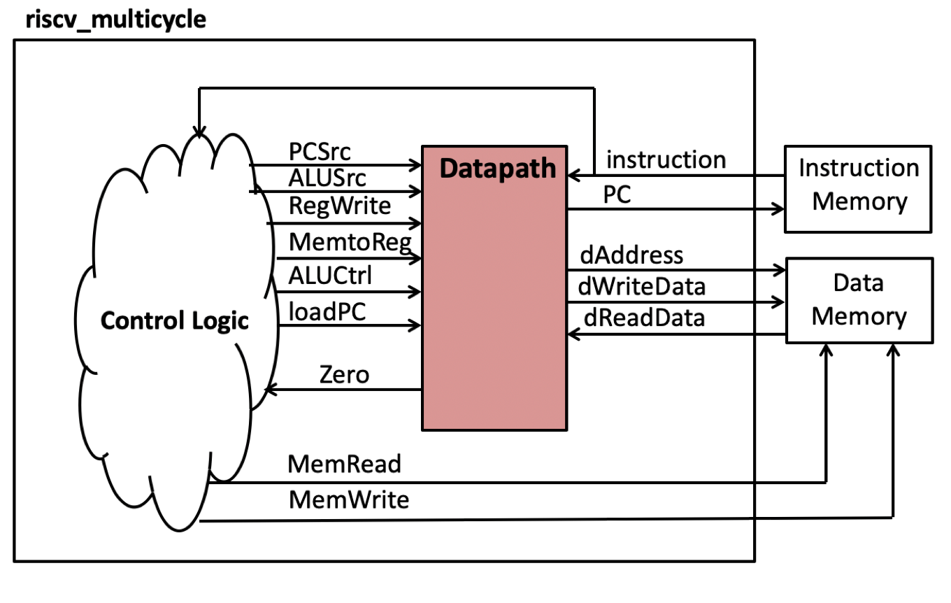
Attach the following ports in the datapath module to their corresponding top-level port within this new module:
- PC
- instruction
- dAddress
- dReadData
- dWriteData
The rest of the logic within this module will generate the control signals that control the datapath module and will be described in more detail below.
2. State Machine
Create a five-state state machine that sequences through the following five steps of executing an instruction:
- IF: Instruction Fetch
- ID: Instruction Decode
- EX: Execute
- MEM: Memory Access
- WB: Write Back
The state diagram for this state machine is shown below. The state machine should return to the ‘IF’ state when the synchronous reset is provided.
3. Control Signals
With the state machine created, create the control signals that will control the datapath.
- The signals
ALUSrc,ALUCtrl, andMemtoReg, depend on the current instruction value only. You do not need to use the current processor state to set these signals. - The
PCSrcdepends on the current instruction and thezerosignal. It also does not need to use the current processor state. - The signals
RegWrite,MemRead, andMemWrite. - The
loadPCdepends only on the current processor state (it operates the same for all processor instructions).
As you create the logic for your controller, you may need additional constants in your SystemVerilog code.
If additional constants are needed, add them to the riscv_datapath_constants.sv file in the include directory of your project.
After completing your multi-cycle controller, add the following files from your previous labs to the project:
- lab05/riscv_simple_datapath.sv
- include/riscv_datapath_constants.sv
- lab02/alu.sv
- include/riscv_alu_constants.sv
- lab03/regfile.sv
At this point, it is a good idea to synthesize your design to find obvious errors and issues before proceeding with simulation. You do not need to report your results at this point but should resolve any errors or significant warnings. Do not proceed to the next exercise until your synthesis problems have been resolved.
Exercise #2 - Testbench #1 “Simulation without Memory”
For this exercise, you will simulate your datapath and control using a testbench that simulates a memory to test if your datapath and control work correctly together. This testbench will do some directed instruction tests.
Add the following testbench file to your project in the ‘sim_1’ simulation set: tb_multicycle_control.sv.
Simulate your testbench with your controller until you have no errors in the testbench (i.e., you get the “Simulation done” message).
Answer the questions in the lab report concerning the testbench simulation
Exercise #3 - Testbench #2 “Simulation with Memory”
In this exercise you will use a second testbench that simulates the processor executing instructions from a simulation instruction memory. In this testbench, your processor will execute its first real program!
Create a new simulation “set” for this different approach for the testbench:
create_fileset -simset sim_2
Add the same tb_multicycle_control.sv testbench that you used for the previous exercise to this new simulation set.
We need to change a parameter in this testbench so that in this simulation set we use memory while in the other simulation set we do not use memory.
Change the parameter for this simulation set as follows:
set_property generic USE_MEMORY=1 [get_filesets sim_2]
Unlike the previous simulation testbench, this testbench simulates the instruction memory (which holds the program memory) and the data memory. The instruction memory is located at the default address of the .text segment (0x00400000). The data memory is located at the default address of the .data segment (0x10010000). Before running the testbench you need to define the initial contents of these memories with a memory data file. You will use the following instruction memory file and data memory files for use in your testbench simulation:
testbench_inst.txttestbench_data.txt
These files were assembled from the following file: testbench.s.txt
Like regular SystemVerilog files, you can add text memory files to your ‘sim_2’ simulation set. Vivado will copy these files to the simulation set and use them during the simulation. You can add them as simulation files with the GUI 1 or you can add them with the following command:
add_files -fileset sim_2 -norecurse {testbench_inst.txt}
You need to explicitly look for “all files” so the GUI doesn’t filter out non design files.
Run this simulation in Vivado. Resolve any errors until you get the “Simulation done” message.
Answer the questions in the lab report concerning the testbench simulation
Exercise #4 - Synthesis
The final exercise in this lab is to synthesize your single-cycle RISC-V control unit.
Summarize the estimated resources for your synthesized logic in the table below. Note that you will have a warning that you are using too many I/Os. This is ok since we are not downloading a bitstream for this lab.
| Resource | Estimation |
|---|---|
| LUT | |
| LUTRAM | |
| FF | |
| IO | |
| BUFG |
Pass Off
To create your submission, make sure the following files are committed in your ‘lab06’ directory:
- riscv_multicycle.sv
Make sure you do not add unnecessary files (including Vivado project files) to your repository.
Test your submission by running the lab06_passoff.py pass-off script found in the starter code.
Review the instructions for submitting and passing off labs to make sure you have completed the lab properly.
Include the following information at the end of your laboratory report.
How many hours did you work on the lab?
Provide any suggestions for improving this lab in the future
-
By default, the GUI will not list the .txt files as available to add to your project when you browse the directory for your memory file. ↩