Table of Contents
Lab #5 - RISC-V Datapath
For this laboratory you will design the simplified datapath for the RISC-V processor in SystemVerilog. Your dataflow implementation will be used in the next lab where you will design the controller for this datapath. Since the data path is only a piece of the processor, you will not be generating a bitfile for this lab and will not be downloading to your FPGA board.
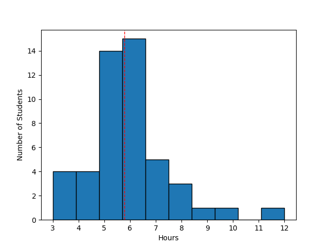 Avg Hours: 5.8, 5.7, 5.4 (Winter 2023, 2022, 2021)
Learning Outcomes
- Understand the low-level implementation of the RISC-V datapath in Verilog
- Verify the operation of your datapath with the Verilog
Preliminary
The internal structure of the RISC-V processor is described in detail in Sections 4.3 - 4.4 of the textbook. You will need to understand this section of the book in great detail to complete this lab. You will likely need to refer to these sections of the textbook as you complete this lab. Make sure you have access to your textbook while completing this lab. The preliminary section of this lab will ask you a number of questions to help you understand the RISC-V instruction format and datapath sufficiently so you can build the datapath in Verilog in the following exercises.
RISC-V Instruction Format
Because your Verilog circuit will be decoding RISC-V instructions, it is essential that you understand how to properly decode and interpret the binary RISC-V instructions. The following questions will test your understanding of the RISC-V instruction format to help you prepare for your datapath design.
You will find the The RISC-V Instruction Set Manual helpful when completing the preliminary and the Verilog for your datapath. The instruction set table will be especially useful and is found on pages 129-136 (pdf pages 147-154).
Immediate ALU Instructions
The table below includes several 32-bit binary values that represent RISC-V instructions with immediate operands. Complete the table by determining (1) the instruction mnemonic, (2) the rs1 field, (3) the rd field, (4) the 32-bit sign extended hexadecimal immediate value contained within this immediate instruction, and (5) the decimal representation of this number. One instruction has been given to you for an example.
Complete the Immediate Instruction Table on learning suite
| 32-bit instruction | neumonic | rs1 | rd | 32-bit Immediate (hex) | Immediate (dec) |
|---|---|---|---|---|---|
| 0xff918113 | addi | 3 | 2 | 0xfffffff9 | -7 |
| 0x01922193 | |||||
| 0x0ff17213 | |||||
| 0xf9c22193 | |||||
| 0x7ff0c293 |
What is the opcode for the ‘addi’ immediate instruction? Provide your answer as a verilog binary constant.
Branch Instructions
The table below contains several conditional branch instructions for the RISC-V. It also contains hypothetical values for the program counter (PC) when the branch instruction is executed. Complete the table by determining (1) the branch type, (2) the 32-bit hexadecimal branch offset in hexadecimal encoded in the instruction, (3) the decimal representation of this number, and (4) the branch target (based on the current PC).
Complete the Branch Instruction Table in learning suite
| 32-bit instruction | Current PC | Branch Type | Offset (hex) | Offset (dec) | Branch Target |
|---|---|---|---|---|---|
| 0x02600c63 | 0x00000004 | beq | 0x00000038 | 56 | 0x0000003C |
| 0xfe139ee3 | 0x00000008 | ||||
| 0x01bfd263 | 0x00000020 | ||||
| 0xfe5a42e3 | 0x000000c4 |
Note: Figure 2.18 in the textbook has the incorrect opcode for branch instructions. Use the Green card or other resource to decode branch instructions.
What is the opcode for Branch instructions?
Exercises
Before proceeding with your laboratory exercises, update your repository with the latest lab starter code.
Exercise #1 - RISC-V Datapath Review
A high-level diagram of the RISC-V processor that you will be designing is shown in the figure below. This diagram contains the following four components:
- Instruction Memory: An addressable memory that contains the instructions that implement the program being executed (the .text segment). Data is only read from this memory.
- Data Memory: An addressable memory that contains the user data (the .data segment). It contains the stack and all the user data used by the program. Data is read from and written to this memory.
- Control Unit: Controls the operation of the datapath.
- Datapath: The internal functional units, registers, and muxes used to implement individual instructions. This is the module you will create for ths lab.
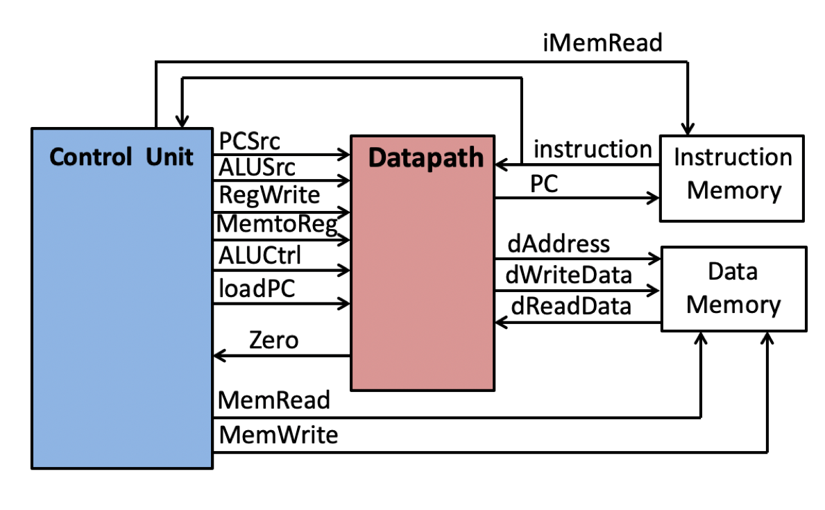
You will be designing the datapath unit in this lab and the control unit in the next lab. You will not be designing the instruction memory and the data memory - they will be provided for you inside of the testbench. A more detailed diagram of these components is shown in Figure 4.21 of the textbook. When you are completed with this lab, your datapath will be able to support the following instructions:
- Register-Register: add, sub, and, or, xor, slt, sll, srl, sra
- ALU Immediate: addi, andi, ori, xori, slti, slli, srli, srai
- Memory: lw, sw
- Branch: beq
Control Signals
Between the control unit and the datapath and memories are a number of signals. The signals going from the control unit to the datapath and memories are called control signals and are used to control the operation of an instruction. The control unit will decode an instruction and then set these control signals in a manner that causes the datapath and memories to execute the appropriate functionality. These control signals are highlighted by the blue signals in Figures 4.21 and 4.23-4.25 of the textbook. It is essential that you understand the purpose of each of these signals.
Determine the purpose of the PCSrc, ALUSrc, RegWrite, MemtoReg, MemRead, and MemWrite signals in the lab report.
Different instructions require different values for the control signals. Determine the value of each control signal for each of the following instructions.
Complete the table in the lab report. Assume the zero signal is ‘0’ for this exercise.
| Instruction | PCSrc | ALUSrc | RegWrite | MemtoReg | MemRead | MemWrite |
|---|---|---|---|---|---|---|
| bne | ||||||
| ld | ||||||
| addi | ||||||
| sd | ||||||
| or |
What is the purpose of the Zero status signal that goes from the datapath to the control unit?
Complete the table below by describing what type of instruction is executing in the datapath for each of the following conditions.
Use the ALU constants from Lab 2 to determine the instruction that is being executed according to the control signals provided. i.e. add, xori, beq (don’t use nop or any pseudo instruction).
| PCSrc | ALUSrc | RegWrite | MemtoReg | MemRead | MemWrite | ALUCtrl | instruction |
|---|---|---|---|---|---|---|---|
| 0 | 0 | 1 | 0 | 0 | 0 | 0000 | |
| 0 | 0 | 1 | 0 | 0 | 0 | 0001 | |
| 0 | 0 | 1 | 0 | 0 | 0 | 0010 | |
| 0 | 0 | 1 | 0 | 0 | 0 | 0110 | |
| 0 | 0 | 1 | 0 | 0 | 0 | 0111 | |
| 0 | 0 | 1 | 0 | 0 | 0 | 1101 | |
| 0 | 1 | 1 | 0 | 0 | 0 | 0010 | |
| 0 | 1 | 1 | 0 | 0 | 0 | 0111 | |
| 0 | 1 | 1 | 0 | 0 | 0 | 0001 | |
| 0 | 1 | 1 | 0 | 0 | 0 | 0000 | |
| 0 | 1 | 1 | 0 | 0 | 0 | 1101 | |
| 0 | 1 | 1 | 1 | 1 | 0 | 0010 | |
| 0 | 1 | 0 | 0 | 0 | 1 | 0010 | |
| 0 | 0 | 0 | 0 | 0 | 0 | 0110 | |
| 1 | 0 | 0 | 0 | 0 | 0 | 0110 |
Note: the last two functions are conditional ‘branches’ but they do not behave the same. Try to identify the operational differences between these two branches.
Exercise #2 - Verilog Datapath
For this exercise you will implement the datapath portion of the processor as shown in the high-level diagram above and described in the textbook. You will complete the control unit in the following lab. Your implementation will need to include the ALU you created in lab #2 and the register file you created in Lab #3. You will also need to add ‘include directories’ to your project so that your project can access the header file you created in lab 2. The following tutorial describes how to add include directories to your project.
Begin your exercise by creating an empty Verilog module in a file named riscv_simple_datapath.sv with the top-level ports summarized in the table below.
The purpose of these control ports will be described later. Note: make sure you follow all ECEN 323 coding standards as you complete your code.
| Module Name: riscv_simple_datapath | |||
|---|---|---|---|
| Parameter | Width | Default Value | |
| INITIAL_PC | 32 | 0x00400000 |
| Port Name | Direction | Width | Function |
|---|---|---|---|
| clk | Input | 1 | Global clock |
| rst | Input | 1 | Synchronous Reset |
| instruction | Input | 32 | Instruction data from Instruction Memory |
| PCSrc | Input | 1 | Source of the PC |
| ALUSrc | Input | 1 | Source of the 2nd operand of the ALU |
| RegWrite | Input | 1 | Write data in the register file |
| MemtoReg | Input | 1 | Register File input multiplexer |
| ALUCtrl | Input | 4 | Indicates which operation that the ALU should perform |
| loadPC | Input | 1 | Update the PC with a new value |
| PC | Output | 32 | Program Counter |
| Zero | Output | 1 | ALU zero indicator |
| dAddress | Output | 32 | Address for data Memory |
| dWriteData | Output | 32 | Data to write into data memory |
| dReadData | Input | 32 | Data read from data memory |
| WriteBackData | Output | 32 | WriteBack data going back into the register file |
Note that your module will need to include a parameter named INITIAL_PC that is used to set the initial value of the PC.
To complete this lab, you will need to know how to add parameters to a System Verilog module.
While creating your datapath module you will need to declare a number of constants related to decoding RISC-V instructions.
You will use these constants throughout your code and will likely use these constants in the next lab.
Create a new file named riscv_datapath_constants.sv that declares these constants and place them in the include directory like lab2. Here is a review on how to setup and use constants from external files like riscv_datapath_constants.sv. Include this file in your datapath module as described in Lab #2.
The remaining description in this exercise will guide you through the process of designing the datapath in Verilog. This design will be organized into the following pieces:
- Program Counter
- Register file
- Immediate Generation
- ALU
- Memory Interface
- Branch Target
- Write Back
The purpose of the datapath is to receive an instruction, decode the instruction (recognize the instruction type and instruction fields) to set the operands of the alu appropriately (for example the alu operand signals will be different from an ADD instruction and SW instruction) then feed in the control signals (which are given in the module ports) where necessary. The green RISCV sheet shows the format for each instruction type so part of this lab is creating/matching System Verilog signals that help define the alu operands with parts of the instruction. For example, the opcode of an instruction could be represented something like this:
logic [6:0] opcode;

assign opcode = instruction[OPCODE_MSB:OPCODE_LSB];
.
.
Since there are multiple instruction formats that use an immediate field differently, you might create a signal to represent each type like:
logic [31:0] immI, immS, immSB;

// sign extension by replicating MSB and concatenating with the immediate
assign immI = {IMM_I_EXT_BITS{instruction[IMM_I_MSB]},instruction[IMM_I_MSB:IMM_I_LSB]};
.
.
Notice in the examples above that there are localparam constants being used when performing the bit slicing of the instruction (for example instruction[OPCODE_MSB:OPCODE_LSB] instead of instruction[6:0]). In most situations, it’s unnecessary to have localparams define constants when performing bit slicing but decoding an instruction is a good example of when to use constants with bit slicing to improve readability. These constants should be added to riscv_datapath_constants.sv. If you do not use localparam constants when doing bit slicing on an instruction as demonstrated above, you will get docked points for this lab.
Complete each of these pieces in order as described below.
1. Program Counter
The first component of the datapath is the Program Counter or PC. The PC is a register that holds the value for the instruction memory address. It points to the location in the instruction memory where the currently executing instruction is located.
Note that your Verilog module must support the parameter “INITIAL_PC”.
This parameter is used to set the initial value of the PC when the datapath is reset with the synchronous rst signal.
The default value is “0x00400000” which is the default value of the .text segment for a RISC-V processor.
As you may remember from ECEN 220, parameters can be added to Verilog modules that allow other modules (such as testbenches) to change the initial value of the PC.
Make sure your PC register is reset with the value of the INITIAL_PC parameter.
The input control signal loadPC is used to indicate that the PC should be updated at the next clock edge.
When this signal is high the PC should be updated with one of two different values:
- PC+4 (when the program proceeds to the next instruction in memory), and
- PC + branch_offset (when the program is taking a branch)
The decision on which of these two choices is loaded into the PC is dictated by the PCSrc control signal (see Figure 4.16 for an explanation on what to do for this control signal). The details of the branch offset will be described below.
2. Register File
At the heart of the datapath is the register file that contains the 32 integer processor registers.
Add the register file from Lab 3 to your datapath.
You will need to create decoding logic that determines the values to the address ports of the register file (i.e., readReg1, readReg2, and writeReg) from the instruction ready from the instruction memory (i.e., the top-level instruction input).
The register write signal should be connected to the top-level RegWrite control input (it will be controlled by the controller module completed in the next lab).
You will attach the other ports later when more logic is added to your datapath.
3. Immediate Generation
For I-type (immediate) instructions, the source of data that enters the second read port of the ALU is the upper 12 bits of the instruction word (instruction[31:20]) that is sign-extended into a 32-bit data value. Create a new signal in your datapath that creates the 32-bit sign extended value for the immediate data for use by the ALU.
You will also need to generate an immediate value for S-type (store) instructions from the instruction read from the instruction memory. The S-type immediate value is different from the I-type immediate value and will thus need a separate signal.
4. ALU
The next major component of the datapath is the Arithmetic Logic Unit (ALU).
You should instance the ALU from Lab 2 into your datapath circuit.
The input to the first ALU operand (op1) is the output from the readData1 port from the register file.
The second operand to the ALU can come from one of two sources: from the second read data port of the register file (readData2) or the immediate sign extended data created from the instruction as described above.
The ALUSrc control signal dictates which input to use (see Figure 4.11 for an explanation on what to do for this control signal).
Create a multiplexer that selects between these two signals and drives the op2 input of your ALU. Attach the top-level ALUCtrl signal to the alu_op input of the ALU module.
As described in the textbook, the Zero signal is used to indicate when the result of the ALU is zero.
This signal is used to decide when branches are taken.
5. Memory Interface
Figure 4.11 shows an instruction memory as part of the datapath. However, you will not need to place the instruction memory in your datapath. The instruction memory will be placed in the testbench for you and your datapath will properly talk to the instruction memory as long as you name your signals correctly in the ports of your module interface. You do not need to do anything for the instruction memory shown in Figure 4.11 of the datapath.
Figure 4.11 also shows a data memory. Just like the instruction memory, you will not need to place the data memory in your datapath. The data memory will be placed in the testbench for you and your datapath will properly talk to the data memory as long as you name your signals correctly in the ports of your module interface.
Although you do not need to add a data memory into your datapath, you do need to generate logic to interface to the data memory.
In particular, you need to determine the values of the signals dWriteData and dAddress.
As shown in Figure 4.11 in the textbook, the memory that is written to the data memory (dWriteData) is the value of the second read port from the register file.
The address for the data memory (dAddress) is the result of the ALU operation.
6. Branch Target
The datapath logic needs to determine the branch target address used when a branch is taken.
The branch target is computed by adding the current value of the PC to the ‘branch offset’ computed by decoding the instruction (SB instruction format).
Note that the branch offset references half-words meaning that the offset should be left shifted by 1 (it cannot encode odd addresses - see page 115).
Implement the System Verilog code needed to compute the branch offset.
Also, create the branch target signal by adding this branch offset to the current PC.
This branch target is loaded into the PC as described above.
7. Write Back
The last piece of the datapath is the write back logic that determines what value is written into the register file.
The value written into the register file is one of two values: the ALU result for conventional arithmetic and logic instructions or the result of the memory read (dReadData).
The MemtoReg control signal dictates which of these two signals is used by the register file (see Figure 4.11 for an explanation on what to do for this control signal).
Create a multiplexer that selects between these two signals and attach the output of the multiplexer to the writeData input of the register file.
The data that is being written to the register file also needs to be attached to the WriteBackData output of the circuit.
Synthesis
At this point, you are required to perform a ‘synthesis’ on your design to make sure that everything is hooked up correctly and that there are no major synthesis warnings. Performing synthesis before simulation is sometimes helpful as you get better debug messages and can find major problems before starting the simulation process. You will need to include your datapath file as part of your lab submission. You may have a number of warnings from synthesis. Note Your synthesized design will use more I/O than available on the FPGA. This is okay - we will not be downloading this to the FPGA. Your design must synthesize properly to pass off this lab (the pass off script will run synthesis on your design).
Indicate the estimated number of resources for your initial synthesis.
Exercise #3 - Testbench Simulation
For this exercise, you will simulate your datapath using a testbench to verify that your datapath works correctly.
This testbench will control the control signals of your datapath to simulate instructions executing in your datapath.
This testbench will provide a simulated memory.
The testbench file is located on the ‘lab05’ directory and is named tb_simple_datapath.sv.
Add the testbench to the simulation files and simulate your datapath with this testbench and debug your datapath unit until it passes the testbench.
Answer the questions about the testbench simulation in the learning suite.
Pass Off
To create your submission, make sure the following files are committed in your ‘lab05’ directory:
- riscv_simple_datapath.sv
Place the following file in the include directory of your GitHub repository:
- riscv_datapath_constants.sv
Make sure you do not add unnecessary files (including Vivado project files) to your repository.
Test your submission by running the lab05_passoff.py pass-off script found in the starter code.
Review the instructions for submitting and passing off labs to make sure you have completed the lab properly.
Include the following information at the end of your laboratory report.
How many hours did you work on the lab?
Provide any suggestions for improving this lab in the future