Table of Contents
Lab 3 - Register File
The register file is another important component of any processor system. The register file stores the values of the registers used by the processor. Almost all instructions read from and/or write to the register file. You will create a register file in this laboratory that you will include in your RISC-Processor used in a later lab.
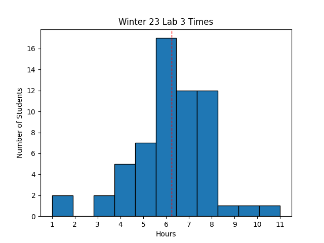 Avg Hours: 6.25, 6.1, 6.1 (Winter 2023, 2022, 2021)
Learning Outcomes
- Understand how multi-ported memories operate
- Be able to create multi-ported memories in SystemVerilog
- Create a synchronous multi-ported register file
Preliminary
All processors include internal registers that are used for performing fast operations in conjunction with the ALU. The register file for the RISC-V processor contains 32x32-bit integer processor registers. The register file you will create in this lab will be reused in future labs and part of your final RISC-V processor.
A number of instructions in the RISC-V instruction set involve reading two values from the register file and writing the result into the register file (i.e., the register instructions). To maximize the speed of executing these instructions it is necessary to read two registers from the register file and write one register into the register file at the same time. A memory that supports the ability to perform more than one read or write during a clock cycle is known as a ‘multi-ported’ memory. The register file you will create will be designed to support the simultaneous reading of two registers and the writing of one register.
The FPGA we are using for the lab includes a dedicated logic element named a “Distributed RAM” that provides the building block for a multi-ported distributed memory. In order to use these memory elements you need to write your SystemVerilog in a very specific manner. If written properly, the synthesis tool will “infer” these special purpose multi-ported memories from your SystemVerilog code. This preliminary will describe how to write your SystemVerilog in a manner that infers these elements. This example is based on the examples provided in the Xilinx Synthesis Guide.
The first step necessary for inferring the multi-ported memory is to declare a multi-dimensional logic array. The following example demonstrates how to declare a memory array that has 8 words and 8-bits wide for each word:
// Declare multi-dimensional logic array (8 words, 8 bits each)
logic [7:0] register[7:0];
The first array index after logic indicates that there are 8 bits in each word.
The second array index after register indicates that there are eight words.
The next step in describing the register file memory is to initialize the memory to all zeros. The multi-dimensional array is initialized using a SystemVerilog ‘initial’ block as follows:
// Initialize the eight words
integer i;
initial
  for (i=0;i<8;i=i+1)
    register[i] = 0;
The final step is to describe the behavior of the memory in an always block.
The code example below demonstrates how to properly describe the memory using a “write-first” mode (i.e., when you write to the same address that you read from, return the new write value rather than the old value).
A detailed description of this code will be given below the code example (note the use of the non-blocking <= operator).
 1: always_ff@(posedge clk) begin
 2:   read1 <= register[addr1];
 3:   read2 <= register[addr2];
 4:   if (write) begin
 5:     register[writeAddr] <= writeData;
 6:     if (addr1 == writeAddr)
 7:         read1 <= writeData;
 8:     if (addr2 == writeAddr)
 9:         read2 <= writeData;
10:   end
11: end
An always_ff block is used in line 1 with the global clock.
This suggests that this memory is synchronous meaning that it operates synchronously with the global clock.
All reads and writes will occur at positive clock edges rather than with some other asynchronous control signal.
Lines 2&3 demonstrate how to access elements of the two dimensional array.
Two accesses are performed simultaneously on the two-dimensional register signal: one is indexed with the signal addr1 and the other with the signal addr2.
Because there are eight elements of the array, both addr1 and addr2 should be three bits in size (thus allowing these signals to select any of the eight words in the array).
The result of these accesses are assigned to the signals read1 and read2.
These signals should be 8 bits as each word in the array is 8-bits wide.
Lines 4-9 define the write behavior of the memory.
If the single-bit write control signal is ‘1’, then the 8-bit signal writeData will be written to the element of the register array specified by the 3-bit signal writeAddr (see line 5).
Lines 6-9 handle the case when one or both of the read ports are reading from the same address that is being written to.
If this is the case, then the corresponding read value is updated with the new writeData rather than the old value that was read in lines 2-3.
Answer the questions in learning suite regarding the behavior of this memory.
The waveform below demonstrates the operation of this multi-ported memory. All memory locations have been initialized to zero. During clock cycle 0, ‘addr1’ and ‘addr2’ both have the value 0 indicating that the value of address 0 will be read from both ports. The result of these reads show up during clock cycle 1 (a value of ‘00’ is read from both ports since all locations are initialized to zero). The ‘write’ signal is low during this clock cycle so no writes occur on the positive clock edge at the end of clock cycle 0.
In clock cycle 1, the ‘write’ signal is asserted to indicate that the value ‘a5’ (on ‘writeData’) will occur to address ‘3’ (‘writeAddress’). This write will occur on the rising edge of the clock at the end of clock cycle 1. The value of the memory at address 1 is read from Port 1 and the value of the memory at address 2 is read from Port 2. Both of these values are 0 and appear during the next clock cycle.
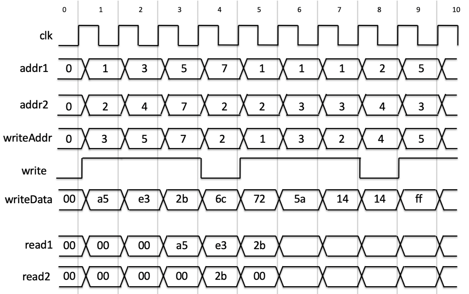
Demonstrate your understanding of the operation of the multi-port memory by completing the waveform above in the learning suite exam.
Exercises
Before proceeding with your laboratory exercises, update your repository with the latest lab starter code.
Exercise #1 - Register File
In this exercise you will create a register file module that you will use within another top-level module in this lab and for your RISC-V processor in later labs of the course.
Begin this exercise by creating a new SystemVerilog file named regfile.sv (within the lab03 directory of your repo) and add the following ports to this module:
| Module Name: regfile | |||
|---|---|---|---|
| Port Name | Direction | Width | Purpose |
| clk | Input | 1 | Global clock |
| readReg1 | Input | 5 | Address for read port 1 |
| readReg2 | Input | 5 | Address for read port 2 |
| writeReg | Input | 5 | Address for write port |
| writeData | Input | 32 | Data to be written during a write |
| write | Input | 1 | Control signal indicating a write |
| readData1 | Output | 32 | Data read from port 1 |
| readData2 | Output | 32 | Data read from port 2 |
After creating the empty module, implement a 32x32-bit register file based on the code examples given in the preliminary. The primary difference between the preliminary example and the register file you should create is that the preliminary example only contained 8 words in the register file and the words were 8-bits.
You will need to submit the file ‘regfile.sv’ inside of your repository.
How many total bits are there in this register file?
Important: There is one other change that you must make in your register file to use it within the RISC-V processor.
You need to add logic that will make sure that address 0 is never written to (i.e., register x0). Register 0 (x0) is always the constant 0 and any writes to this register that change the value will cause problems when executing RISC-V code.
To prevent address 0 from being written, add additional logic that only allows a write to the register file to occur when (1) the write signal is asserted and (2) writeReg!=0.
After creating your register file, create a tcl simulation file named regfile_sim.tcl and simulate the reading and writing of your register file.
Your tcl simulation must perform the following:
- Write to two different registers (not x0). Write a negative value to one register and a positive value to the other
- Write a non-zero value to register x0
- Read the three registers you wrote to (making sure that you read a 0 from x0)
You will need to submit your simulation regfile_sim.tcl file as part of your “Pass Off” below.
Exercise #2 - Registerfile Testbench
The simulator and waveform viewer are very important tools that you will use throughout the semester. The better you know how to use these tools the more effective and efficient you will be in completing the labs in this class. When simulating with a testbench, only the top testbench signals show up in the simulator. You will be interested in looking at the signals in your circuit to make sure your circuit is working correctly. Review the Simulation Tutorials to learn how to add your module signals in the simulator and other simulation tips and techniques.
Answer the questions in the lab report regarding the simulation tools.
Because your register file will be used within several processors in later labs, it is essential that the register file is fully tested.
For this exercise you will simulate your register file with the tb_regfile.sv testbench provided in the starter code.
This testbench will simulate a large number of cases to make sure it is working properly for this lab and future labs.
Create a new simulation set named sim_2 and add the tb_regfile.sv testbench to this simulation set as described in the previous lab.
Simulate and debug your circuit until you get a successful simulation.
An example of a successful simulation is shown below:
*** Start of Regfile Testbench Simulation ***
relaunch_sim: Time (s): cpu = 00:00:00 ; elapsed = 00:00:18 . Memory (MB): peak = 1095.965 ; gain = 0.000
run all
*** Testing x0 register at time 140 ns
*** Testing write to each register at 830 ns
*** Testing simultaneous reads and writes to each register at 1500 ns
*** Testing different read addresses at 1860 ns
*** Testing random transactions at 2180 ns
*** Successful simulation. Ended at 5670 ns ***
Answer questions about the testbench results in learning suite.
Exercise #3 - Regfile Top Circuit
For this exercise, you will create a top-level circuit that uses both your register module and the alu module you created in the previous lab.
The top-level circuit you will create is a simple dataflow circuit that is similar to the RISC-V datapath circuit you will create in lab 5.
This circuit will allow you to store values in the register file and perform ALU operations on the values stored in the ALU much like the RISC-V processor.
The difference is that you will need to control the operation of the ALU and register file with buttons and switches manually to simulate the operation of the processor controller.
The following discussion will describe the circuit and then describe how to control the circuit.
Begin by creating a new file named regfile_top.sv with the module named regfile_top and add the following top-level ports:
| Module Name: regfile_top | |||
|---|---|---|---|
| Port Name | Direction | Width | Purpose |
| clk | Input | 1 | Global clock |
| btnc | Input | 1 | Center Button - Write register |
| btnl | Input | 1 | Left Button - Load address register |
| btnu | Input | 1 | Up Button - Global Reset Signal |
| btnd | Input | 1 | Down Button - Multiplexer select signal |
| sw | Input | 16 | Switches for data input |
| led | Output | 16 | LEDs for accumulator output |
This circuit will combine the ALU you created in the previous lab with the register file you created in the previous exercise. This circuit will allow you to perform basic ALU and register operations by setting the switches and buttons and looking at the results on the LEDs. You will be able to load any value into any register in the register file and you will be able to perform any of the ALU operations on the data in the register file and store the results back into the register file. The diagram below describes the architecture of this circuit.
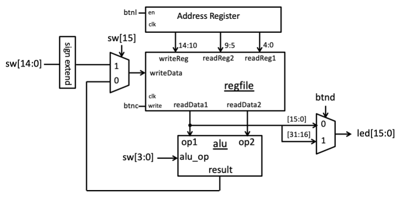
Address Register
Begin by creating a 15-bit register that controls the three ports of the register file. This register should be reset by the global reset signal (‘btnu’) and loaded with the bottom 15 switches (sw[14:0]) when ‘btnl’ is pressed. The 15 bits of the address register will be used to control the address of the three ports of the register file as follows:
- bits[4:0] - the register address for the first operand (readReg1 port)
- bits[9:5] - the register address for the second operand (readReg2 port)
- bits[14:10] - the register address for the destination register (writeReg)
Register File
Next, instance your register file and hook up the address ports of the register file to the address register as described above.
The write signal used to write a new value into the register file should be set when ‘btnc’ is pressed.
You will need to create a synchronizer and one-shot circuit to prevent this signal from being asserted more than once when the button is pressed.
The signals going to the other ports of the register file will be described below.
ALU
Add your ALU from lab 2 to your project (do not copy the file to lab 3 - just reference your code from lab 2).
Attach your ALU to your design as shown in the diagram above.
Specifically, attach the output of the readData1 signal on the register file to the op1 input of the alu and attach the output of the readData2 signal on the register file to the op2 input of the alu.
All operations performed by the ALU will be between the values found in the register file.
The ‘alu_op’ input of the ALU should be driven by switches [3:0].
Write Data
The input to the writeData signal is driven by a multiplexer that chooses between the two types of operations.
When sw[15]=0, this multiplexer will pass the ALU result to the writeData (i.e., the output of the ALU will be written into the register file).
When sw[15]=1, the multiplexer will pass a 32-bit sign-extended value of the lower 15 switches.
Begin by creating a 32-bit sign-extended value of the lower 15 switches.
Next, create a multiplexer that chooses between the output of the ALU and the 32-bit sign extended value.
Attach the output of this multiplexer to the writeData input of your register file.
LED Outputs
The final step in creating the circuit is to attach the LEDs.
Create a multiplexer that selects the lower 16-bits of the readData1 when ‘btnd’ is NOT pressed and selects the upper 16-bits of the readData1 signal when ‘btnd’ IS pressed.
This will allow the user to examine the full 32-bit value of readData1.
A one shot is not needed for ‘btnd’.
Controlling the Datapath Circuit
If you have created your circuit, you will need to test it with a TCL file to demonstrate the top-level register file. The notes below describe how a user (and your TCL file) will perform operations on this circuit.
Step 1: Set Address Register
The first step in performing an operation is to set the ‘Address Register’. The address register holds three different addresses: an address for the first source operand, an address for the second source operand, and address for the result destination. To set the value of the address register, the user will set the switches as follows:
- sw[4:0] - the register address for the first operand (readReg1 port)
- sw[9:5] - the register address for the second operand (readReg2 port)
- sw[14:10] - the register address for the destination register (writeData)
For example, if a user wanted to perform an operation between register x1 and x3 and store the result in x5, the user would set switches [4:0] to ‘00001’ to indicate register x1 for operand 1, switches [9:5] to ‘00011’ to indicate register x3 for operand 3, and switches [14:10] to ‘00101’ to indicate that the result should be stored in register x5. Concatenating these signals together, the user would set the switches to ‘001010001100001’ (note that switch 15 will be set in the next step).
After setting the switches to indicate the source operand addresses and the destination address, the user would press ‘btnl’ to load the address register with this value.
Step 2: Set Operation Control
The second step in performing an operation is to indicate what type of operation to perform with the register data. There are two types of operations: conventional ALU operations and a load value operation with the switches. The ALU operation type is determined by switch 15. If switch 15 equals 0 (sw[15]=0) then a conventional ALU operation will be performed, if switch 15 equals 1 (sw[15]=1), then a new value indicated by the switches is loaded into the register file. Each of these operation types are described below.
ALU Operation
To perform an ALU operation, sw[15] should be set to zero. Next, the ALU operation that is to be performed should be set on switches[3:0]. The constants for the ALU operation were defined in the previous lab. For example, if the user wants to perform an ‘addition’ between two operations, sw[3:0] should be set to ‘0010’ to indicate an addition operation. Any of the ALU operations supported by your ALU can be executed.
New Value Load Operation
To load a new value into a register, sw[15] should be set to on (sw[15]=1). The other 15 switches should be set to the signed value to be loaded into the destination register. This 15-bit number will be sign extended to 32-bits and loaded into the destination as specified in the address register. For example, if the number 693 is to be loaded into a register, the switches [14:0] are set to “000001010110101” and sw[15]=’1’.
Step 3: Perform Operation
After the address register has been set and the operation specified, the operation is performed when the user presses ‘btnc’.
Example Operation
The following example demonstrates how to perform the operation x3=43+27.
The following three operations must be executed on the system to complete this operation:
1:x1 = 43
2:x2 = 27
3:x3 = x1 + x2
Each operation is composed of two phases: the load address phase and the operation phase. The following table demonstrates what buttons and switches must be set to complete this operation:
| Step | Switches | Buttons | Note |
|---|---|---|---|
| 1a | 0 00001 00000 00000 (0x0400) | btnl | Load 1 into write address (0 in others) |
| 1b | 1 000 0000 0010 1011 (0x802b) | btnc | Load constant 43 into register 1 |
| 2a | 0 00010 00000 00000 (0x0800) | btnl | Load 2 into write address (0 in others) |
| 2b | 1 000 0000 0001 1011 (0x801b) | btnc | Load constant 27 into register 2 |
| 3a | 0 00011 00010 00001 (0x0c41) | btnl | Load 3 into write address, 1 in A port address, 2 in B port address |
| 3b | 0 00000000000 0010 (0x0002) | btnc | Perform Addition Operation |
Demonstrate your understanding on how to control this datapath by determining the values of the buttons and switches necessary to complete the operation listed below:
1:x7 = -35
2:x9 = x0 ^ x7
3:x15 = x7 & x9
| Step | Switches | Button |
|---|---|---|
| 1a | ||
| 1b | ||
| 2a | ||
| 2b | ||
| 3a | ||
| 3b |
Complete the table on learning suite.
After creating your top-level circuit, simulate your circuit with a tcl script named regfile_top_sim.tcl.
This tcl script should simulate your circuit as follows:
- Write the value 0x00001234 to register 1
- Write the value 0x00003678 to register 2
- Perform an add operation between register 1 and register 2 and store the result in register 3
You will need to submit your simulation regfile_top_sim.tcl file as part of your “Pass Off” below.
In addition to your .tcl simulation, you will need to simulate your top-level register file with a top-level testbench.
Create a new simulation set that includes the tb_regfile_top.sv testbench from your starter code.
This testbench will simulate button presses and switches to check to see that your top-level register file circuit is working properly.
This testbench will print a number of messages during the execution of your circuit and provide a message indicating that it has passed the testbench.
Exercise #4 - Implementation and Download
In this final exercise, you will go through the steps required to synthesize, implement, and generate a bitstream for your top-level register module.
To proceed with the implementation of your top-level register file circuit create a new ‘.xdc’ constraints file named regfile_top.xdc to map the top-level I/O of your circuit to actual pins on the Basys3 board.
When you have completed this file, add this as a constraint file to your Vivado project.
After creating this file and adding it to your project, you can proceed with the synthesis, implementation, and bitstream generation steps of this process.
Indicate the number of resources consumed by this design and the WNS in the laboratory report.
Note: If your register file circuit was synthesized properly, it should allocate some “LUTRAM” elements. If you do not have LUTRAM primitives in your synthesized design then there is a problem and you should work with a TA or instructor to resolve it before proceeding.
Download
Once you have successfully generated a bitstream for your top-level register file circuit, download this bitstream to your Basys3 board. Experiment with your circuit and verify that it functions as expected.
Pass Off
To create your submission, make sure the following files are committed in your ‘lab03’ directory:
- regfile.sv
- regfile_sim.tcl
- regfile_top.sv
- regfile_top.xdc
- regfile_top_sim.tcl
Make sure you do not add unnecessary files (including Vivado project files) to your repository.
Test your submission by running the lab03_passoff.py pass-off script found in the starter code.
Review the instructions for submitting and passing off labs to make sure you have completed the lab properly.
Include the following information at the end of your laboratory report.
How many hours did you work on the lab?
Provide any suggestions for improving this lab in the future