Table of Contents
Lab #2 - Arithmetic Logic Unit (ALU)
An Arithmetic/Logic Unit or ALU is an important component of any processor system. This unit is the “brains” of the processor and performs the arithmetic functions such as addition and subtraction as well as logical functions such as AND/OR. You will create an ALU in this laboratory that you will use for your RISC-V processor in a later lab. You will also use this ALU to implement a simple “calculator” on the FPGA.
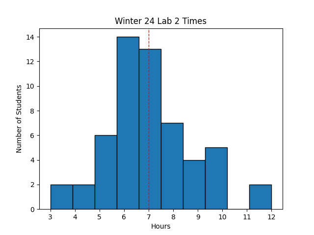 Avg Hours: 7.0, 6.9, 6.5, 5.8 (Winter 2024, 2023, 2022, 2021)
Learning Outcomes
- Apply Hierarchy in a top-level SystemVerilog design
- Create a reusable combinational ALU circuit
- Create top-level ‘calculator’ circuit based on your ALU
- Verify your Calculator circuit with a “testbench” file on the Simulator
Preliminary
The ALU in most processors performs both arithmetic operations (add, subtract, multiply, and divide), logical operations (and, or, not, xor, etc.), and shift operations (shift right, shift left, etc.). All ALU arithmetic operations are performed in binary arithmetic. You should be familiar with all of these operations from your study in ECEN 220. These preliminary exercises will help you review your understanding of binary representation, binary arithmetic, and logical operations. Complete the following questions to demonstrate your understanding of these concepts. You are free to use a calculator, a Verilog simulator, or any other tool to help you complete these questions. Although computing aides to complete these questions are allowed, you may be asked to complete these types of problems by hand for homework or exams.
Binary Representation
It is essential that you are comfortable representing numbers in binary and hexadecimal formats. It is also essential that you are able to convert binary numbers and two’s complement numbers to their decimal equivalents. Answer the following questions to demonstrate your understanding of these concepts. Provide all of your answers as SystemVerilog constants (i.e., <size>’<radix><value>, for example 16’d10 for the 16-bit decimal number 10). Use lower case for all alphabet characters for the learning suite grading tool.
What is the 16-bit hexadecimal representation of the binary number 16’b0100111001101011?
What is the 16-bit binary representation of the hexadecimal number 16’he6c7?
What is the 16-bit two’s complement binary representation of the decimal number 16’d17364?
What is the 16-bit two’s complement binary representation of the decimal number -16’d9702? (note that this is a negative number)
What is the decimal number represented by the two’s complement hexadecimal number 16’h53fc?
What is the decimal number represented by the two’s complement hexademical number 16’9fb0?
Two’s Complement Sign Extension
Signed binary numbers are represented in two’s complement notation. In many situations it is necessary to extend the number of bits of a signed number. Answer the following questions to demonstrate your understanding of two’s complement sign extension.
Use two’s complement sign extension to extend the two’s complement number 8’h38 to a 16-bit two’s complement hexadecimal number.
Use two’s complement sign extension to extend the two’s complement number 8’hf4 to a 16-bit two’s complement hexadecimal number.
Two’s Complement Addition and Subtraction
Demonstrate your understanding of binary addition by answering the following questions. Provide all of your answers as SystemVerilog constants.
Determine the two’s complement addition of each of the following:
-
16’h2f37 + 16’h3ef7
-
16’h9742 + 16’h4fe3
-
16’hfb1a + 16’hb16c
Determine the two’s complement subtraction of each of the following:
-
16’h3ef7 - 16’h2f37
-
16’h9742 - 16’h4fe3
-
16’hfb1a - 16’hb16c
Two’s Complement Operation (Negation)
Two’s complement numbers can be negated by determining the “two’s complement” of the number. Determine the “two’s complement” of each of the following numbers:
-
16’h3ef7
-
16’h9742
-
16’hfb1a
Logical Operations
Demonstrate your understanding of the binary logical operations of AND (&), OR (|), and XOR (^) by determining the result of each logical operation. Provide all of your answers as SystemVerilog constants.
-
16’h3ef7 & 16’h2f37
-
16’h9742 | 16’h4fe3
-
16’hfb1a ^ 16’hb16c
Shift Operations
Demonstrate your understanding of the shift operations by determining the result of each shift operation listed below. Provide all of your answers as SystemVerilog constants.
-
16’h3ef7 << 2
-
16’h9742 >> 5
-
16’h9742 >>> 3
Exercises
Before proceeding with your laboratory exercises, update your repository with the latest lab starter code.
Exercise #1 - Arithmetic and Logic Unit
For this exercise you will design an “Arithmetic Logic Unit” (ALU) for a simplified version of the RISC-V processor. You will use this ALU in your RISC-V processor in a later lab. Your ALU will be designed to implement the following ALU operations signed addition, signed subtraction, logical AND, logical OR, logical XOR, “Less Than” comparison, and three different shift operations. We will talk about the ALU in more detail when we discuss Chapter 4 of the textbook but you are ready to create the ALU with the background you have now.
As you create files for this laboratory, keep all of these files in the lab02 directory of your repository.
All of your files will need to be in this directory as part of the passoff process so you might as well start by keeping the files here and editing them in this directory rather than copying them over from some other directory at the end of the lab.
Begin your module by creating a new SystemVerilog file named alu.sv.
Define a new module named alu and add the following ports (the port names MUST be exact to match with the testbench):
| Module Name: alu | |||
|---|---|---|---|
| Port Name | Direction | Width | Purpose |
| op1 | Input | 32 | Operand 1 |
| op2 | Input | 32 | Operand 2 |
| alu_op | Input | 4 | Indicates which operation to perform |
| zero | Output | 1 | Indicates when the ALU Result is zero |
| result | Output | 32 | ALU Result |
The ALU you are going to create is a ‘32-bit’ ALU meaning that the inputs are 32-bits and produce a 32-bit output. The ALU will perform one of the different operations between the ‘op1’ and ‘op2’ operands based on the value of the ‘alu_op’ input signal.
This circuit is a ‘combinational’ circuit meaning that the circuit output result depends only upon the inputs (‘op1’, ‘op2’, and ‘alu_op’) and there is no memory to store previous state (there are no registers and thus no need for a clock or reset input). The function performed by the alu is based on the four-bit input ‘alu_op’ signal as specified by the following table:
| alu_op | Function |
|---|---|
| 0000 | AND |
| 0001 | OR |
| 0010 | Addition |
| 0110 | Subtraction |
| 0111 | Less Than |
| 1000 | shift right logical |
| 1001 | shift left logical |
| 1010 | shift right arithmetic |
| 1101 | XOR |
The default behavior for values not specified is addition1. Each of the operations are described in more detail below.
Addition
The addition operation performs signed two’s complement addition. Addition is relatively easy using the ‘+’ operator:
result = op1 + op2;
Signed Subtraction
The subtraction operation performs signed two’s complement subtraction (op1 - op2). Subtraction can be implemented simply using the ‘-‘ operator:
result = op1 - op2;
Logican AND
AND is implemented using the ‘&’ operator:
result = op1 & op2;
Logical OR
OR is implemented using the ‘|’ operator:
result = op1 | op2;
Logical XOR
XOR is implemented using the ‘^’ operator:
result = op1 ^ op2;
Less Than (LT)
The ALU must also perform a “less than” operation that returns a ‘1’ if op1 is less than op2 or a ‘0’ otherwise (if op1 is equal to or greater than op2). Implementing the less than operation is a bit more involved in SystemVerilog. In general, Verilog will treat wires and reg signals as unsigned. The Verilog code “A < B” will treat A and B as unsigned numbers. We want this comparison to operate on signed numbers. To account for signed numbers, we need to cast the operands A and B to signed numbers using the “$signed” Verilog command. The following example demonstrates how to modify the example Verilog text code to properly handle comparisons between signed numbers:
result = $signed(op1) < $signed(op2)
Shift
SystemVerilog supports the operators you need for the three types of shifting that must be performed: << for shift left logical, >> for shift right logical, and >>> shift right arithmetic.
The second operator determines how many places to shift the first operator.
Only five bits are needed for the second operand of a shift as five bits allow a shift between 0 and 31 places.
Shifts of 32 or more are corner cases that will result in all zeros or all ones.
Examples of of right and left logical shifting are shown below:
result = op1 << op2[4:0];
result = op1 >> op2[4:0];
To force a proper arithmetic shift when using the >>> operator, you need to cast the value being shifted as a signed number like you did for the ‘less than’ operation and then cast the result back to an unsigned as follows:
result = $unsigned($signed(value_to_be_shifted) >>> op2[4:0])
Zero Output
In addition to performing an arithmetic, logic, or shift operation, the ALU should provide a single-bit output that indicate whether the result is a zero or not. The output signal ‘zero’ should be set to a ‘1’ when the result of the operation is zero and ‘0’ otherwise.
Assuming ‘op1’=32’hf3212f37 and ‘op2’=32’h621c3ee7, determine the value of ALU result for the given value of ‘alu_op’:
- 4'b0000
- 4'b0001
- 4'b0010
- 4'b0011
- 4'b0110
- 4'b0111
- 4'b1000
- 4'b1001
- 4'b1010
- 4'b1101
Note: You may want to create a TCL script to compute these values from your circuit in the simulation step described below rather than compute them by hand.
ALU Multiplexer
Your ALU circuit needs to include a multiplexer to select which of the functions to perform.
A case statement within a always_comb block is the most convenient way to implement this multiplexer (you will be penalized if you do not use a case statement).
You should avoid any hard-coded “magic numbers” in your code (as specified in the class coding standard).
You can specify these constants using the localparam SystemVerilog directive as follows:
localparam[3:0] ALUOP_AND = 4'b0000;
You will need to create a constant for each of these six ALU operation commands.
Since these commands will need to be used by both your ALU and other circuits that instance your ALU, you should create these constants in a separate SystemVerilog header file named riscv_alu_constants.sv.
Place this file in the include directory of your repository so it can be used by this lab and other future labs.
You will also need to add ‘include directories’ to your project so that your project can access search for this file in the include directory.
The following tutorial describes how to add include directories to your project.
Include this header file in your alu.sv SystemVerilog by using the include directive into your alu.sv file:
`include "riscv_alu_constants.sv"
Once you have created your alu circuit, create a tcl file named alu_sim.tcl that simulates all of the operations on the ALU.
To set 32-bit values more conveniently than typing the binary, you can set the values of signals in hex as follows:
add_force op1 ffe123b3 -radix hex
Make sure your TCL file conforms to the class TCL file coding standards as you create your TCL file. Verify manually that your ALU computes the correct result for each of your cases.
You will need to submit your simulation alu_sim.tcl file as part of your “Pass Off” below.
Exercise #2 - ALU Testbench
Simulating with “.tcl” files is useful for short simulations just to see if your circuit is performing basic operations. This type of simulation, however, is usually not sufficient for fully verifying your logic design. A “testbench” SystemVerilog file is often used to more thoroughly test your module. For this exercise, you will continue with the simulation process by using a testbench to test your calculator circuit. For most laboratory assignments in this course you will be provided with a testbench. Since you will be using testbenches extensively in the laboratory assignments it is important to understand how to use testbenches. The ECEN 220 testbench tutorial contains a video that describes how to use a testbench to simulate your module.
In this exercise, you will test your ‘alu’ module with a SystemVerilog testbench file tb_alu.sv.
This file is located in the /lab02/ directory of the lab starter code in your repository.
This testbench instances your alu module and provides a stimulus to the inputs and carefully monitors the outputs.
The testbench will report an error and stop the simulation if it sees an error.
You will need to simulate and debug the testbench with your alu module until you “pass” the testbench (i.e., the simulation exits without any errors).
The Vivado simulator supports the ability to create different simulation environments, called simulation sets, so that you can create different simulation environments within the same project. In the previous exercise you simulated your alu by manually providing a stimulus with a .tcl simulation script. In this environment your alu module was the “top-level” module and stimulus was provided by the script. For this exercise you will need a different environment for your simulation. This environment will use the “tb_alu” testbench as the top-level and this testbench will provide the stimulus.
Simulation environments are called simulation “sets”.
Your .tcl simulation environment from the previous exercise was named sim_1 (by default).
You will need to create a different simulation set, called sim_2, for this testbench simulation environment.
You can use sim_1 to simulate with your .tcl script and sim_2 to simulate with the testbench.
You will create additional simulation environments in the next exercises.
You can create a simulation set named sim_2 by executing the following .tcl command:
create_fileset -simset sim_2
After executing this command, a new simulation set has been created that can be customized to run the testbench.
Add the tb_alu.sv testbench file to the simulation set by either using the GUI (add file ‘+’ icon) or executing the following TCL command:
add_files -fileset sim_2 tb_alu.sv
(Note that you need to either specify the full path of the testbench file or be in the directory of the testbench to run the command shown above.)
The image below demonstrates what your sources window should look like if sim_2 was properly added.
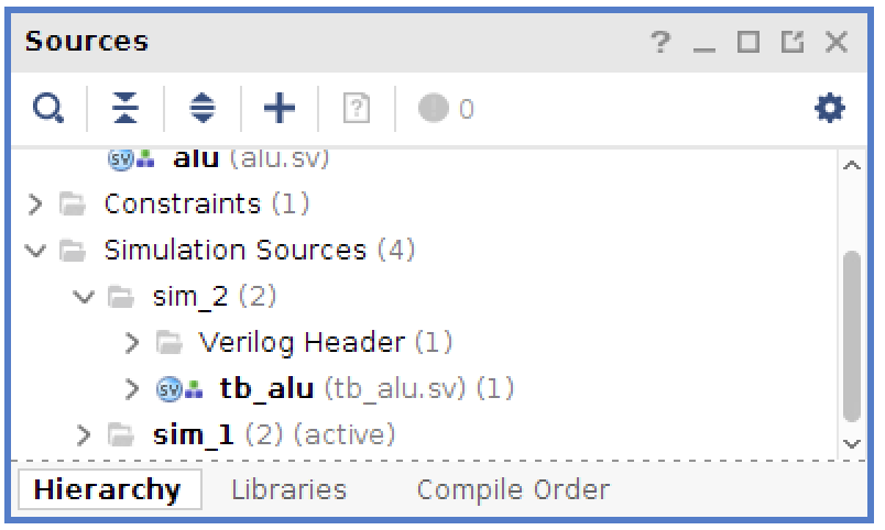
In the figure shown above, ‘‘sim_1’’ is currently active. You can activate either simset by selecting it, right click, and select “Make Active”. Or, you can make it active by executing the following TCL command:
current_fileset -simset [get_filesets sim_2]
Simulate your alu module with the testbench by making sim_2 active and running the simulator.
The testbench has been designed to exit when an error occurs or when the testbench has completed its tests.
You can click the “play” button in the simulator or execute the run -all command on the command line to initiate the testbench simulation.
If you have any errors in your simulation, resolve the errors before proceeding.
An example of the end of the output of a successful run is shown below:
*** Simulation Complete ***
The alu module requires a clock. True or False?
What is the value of operand1 at time t = 220ns?.
What is the value of operand2 at time t = 220ns?.
What operation is the ALU performimng in the testbench at time t = 1090ns?
Exercise #3 - Top-Level Calculator Circuit
For this exercise you will design a top-level calculator circuit that uses the ALU you created in the previous exercise. This circuit will maintain a current value of the “calculator” in a 16-bit accumulator register and allow the user to update the value by implementing any of the arithmetic and logic functions provided by your ALU.
Begin your module by creating a new SystemVerilog file named calc.sv.
Define a new module named calc and add the following ports (the port names MUST be exact to match with the testbench):
| Module Name: calc | |||
|---|---|---|---|
| Port Name | Direction | Width | Purpose |
| clk | Input | 1 | Global clock |
| btnc | Input | 1 | Center Button |
| btnl | Input | 1 | Left Button |
| btnu | Input | 1 | Up Button |
| btnr | Input | 1 | Right Button |
| btnd | Input | 1 | Down Button |
| sw | Input | 16 | Switches for data input |
| led | Output | 16 | LEDs for accumulator output |
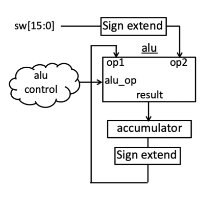
The two key components of the circuit are a 16-bit accumulator to hold the current value of your calculator and the ALU you created in the previous exercise. The relationship of the ALU and the accumulator should be designed as shown in the following figure:
Create a 16-bit register (called the accumulator) to hold the contents of the current value of the calculator.
Use a always_ff@ block for this register.
Design your register as follows:
- The accumulator should be connected to the global clock input
- The accumulator should reset to zero using a synchronous reset when the ‘up’ button (btnu) is pressed
- The input to the accumulator should be the lower 16-bits of the 32-bit result output of the ALU
- The accumulator should be updated once every time the ‘down’ button (btnd) is pressed (use the one shot filter from the previous lab for this)
- Attach the value of the accumulator to the LED outputs
Connect the inputs to the ALU as follows:
- Create a 32-bit signal that is a sign extended version of the 16-bit accumulator. Attach this signal to the ‘op1’ input of the ALU
- Create a 32-bit signal that is a sign extend version of the 16-bit switch inputs. Attach this signal to the ‘op2’ input of the ALU
- Connect the lowest 16-bits of the ‘result’ output to the input of the accumulator (as discussed above)
- Create a new signal for the ‘alu_op’ signal and generate the logic for this signal as discussed below.
You can create a 32-bit sign extended signal using the Verilog ‘concatenation’ operator (i.e., concat the top bit of the signal you are sign extending and replicate it as many times as necessary). Search online about the ‘concatenation’ and ‘replication’ operator to review the syntax of these operators.
The ‘alu_op’ signal determines which ALU operation to perform. You will determine which operation to perform based on the value of the three buttons: btnl, btnc, and btnr. You do not need “one shot” filters for these three buttons since they will be read immediately when ‘btnd’ is pressed. You should create a combinational circuit that generates the proper ‘alu_op’ signal based on the value of these three buttons as follows:
| Module Name: calc | ||||
|---|---|---|---|---|
| btnl | btnc | btnr | Function | alu_op |
| 0 | 0 | 0 | Add | 0010 |
| 0 | 0 | 1 | Sub | 0110 |
| 0 | 1 | 0 | AND | 0000 |
| 0 | 1 | 1 | OR | 0001 |
| 1 | 0 | 0 | XOR | 1101 |
| 1 | 0 | 1 | Less Than | 0111 |
| 1 | 1 | 0 | SLL | 1001 |
| 1 | 1 | 1 | SRA | 1010 |
If you use the constants defined in the riscv_alu_constants.sv file for your top-level design, you also need to include this file in your calc.sv file like you did for the alu.sv file.
You will need to create a combinational circuit that converts the three bit value specified by the three buttons to the corresponding four-bit alu_op value for the ALU. The following table demonstrates how this circuit should operate after setting the buttons and switches:
| btnl,btnc,btnr | Previous Value | Switches | Function | New Value after btnd |
|---|---|---|---|---|
| (Press btnu for reset) | xxxx | xxxx | Reset | 0x0 |
| 0,1,1 | 0x0 | 0x1234 | OR | 0x1234 |
| 0,1,0 | 0x1234 | 0x0ff0 | AND | 0x0230 |
| 0,0,0 | 0x0230 | 0x324f | Add | 0x347f |
| 0,0,1 | 0x347f | 0x2d31 | Sub | 0x074e |
| 1,0,0 | 0x074e | 0xffff | XOR | 0xf8b1 |
| 1,0,1 | 0xf8b1 | 0x7346 | Less Than | 0x0001 |
| 1,0,1 | 0x0001 | 0xffff | Less Than | 0x0000 |
Once you have created your calculator circuit, remove all syntax errors and open the simulator with your top-level circuit.
It may take some iterations in starting the simulator to identify and remove all errors.
Once your circuit is successfully in the simulation and all syntax errors have been removed, simulate your circuit by creating a custom simulation .tcl script.
Create TCL simulation file named calc_sim.tcl that performs the following simulation steps:
- Create an oscillating clock for the input clock
- Press btnu to issue a global reset
- Implement the operations shown in the table above
You will need to submit your simulation calc_sim.tcl file as part of your “Pass Off” below.
Exercise #4 - Calculator Testbench Simulation
In this exercise, you will simulate your calculator with another testbench file named tb_calc.sv that is included with your lab starter code.
Like the testbench used for the alu, this testbench instances your calculator module and provides a stimulus to the inputs and monitors the outputs.
Create another simulation set named sim_3 and add the tb_calc.sv file to this simulation set.
Simulate your calculator circuit until you have removed all errors and successfully pass the testbench.
Note that the pass off script will run this testbench against your submitted design files as part of the pass off process.
Exercise #5 - Implementation and Download
In this final exercise, you will go through the steps required to synthesize, implement, and generate a bitstream for your ‘alu’ module. You will also download the module to the Basys3 board.
.xdc file
To proceed with the implementation of your calculator circuit you will need to create a ‘.xdc’ constraints file named calc.xdc to map the top-level I/O of your circuit to actual pins on the Basys3 board.
You may create this file by modifying the standard resources/Basys-3_323.xdc file in your lab starter code.
To modify this file, uncomment the lines in the file that correspond to pins that you use and make sure the names of your top-level ports match the names listed in the .xdc file.
When you have completed this file, add this as a constraint file to your Vivado project.
After creating this file and adding it to your project, you can proceed with the synthesis, implementation, and bitstream generation steps of this process. You may want to refer to the instructions in Lab 1 to remind you on how to complete these steps.
Indicate the number of resources consumed by this design and the timing (Worst Negative Slack) in the laboratory report.
Download
Once you have successfully generated a bitstream for your calculator circuit, download this bitstream to your Basys3 board. Experiment with your circuit and verify that it functions as expected. A TA will regenerate your bitstream from your submitted repository and validate that it works correctly. You will may lose points on your laboratory submission if your downloaded bitstream does not work as described in the lab.
Pass Off
The final step is to complete the ‘pass off’ as you did in the previous lab.
Prepare your repository by making sure you have all of the following files added to your lab02 directory of your GitHub repository:
- alu.sv
- alu_sim.tcl
- calc.sv
- calc_sim.tcl
- calc.xdc
Place the following file in the include directory of your GitHub repository:
- riscv_alu_constants.sv
Make sure you do not add unnecessary files (including Vivado project files) to your repository.
Test your submission by running the lab02_passoff.py pass-off script found in the starter code.
Review the instructions for submitting and passing off labs to make sure you have completed the lab properly.
Include the following information at the end of your laboratory report.
How many hours did you work on the lab?
Provide any suggestions for improving this lab in the future
-
You may wonder why four bits are needed to encode only nine operations. The four bits may specify up to 16 different operations. The RISC-V can perform a number of other operations that we will not implement in this course. To remain compatible with the description in the textbook we will stick with the four bits and the encoding described in the text. ↩