The Vivado synthesis tool can be run in GUI mode to view the schematic of your design.
This is often useful to check the connectivity and high-level structure of your design.
You can view the schematic in ‘pre-synthesis’ mode (i.e., after HDL elaboration but before synthesizing to FPGA resources) or in ‘post-synthesis’ mode (i.e., after FPGA synthesis where the netlist uses FPGA resources).
This tutorial will describe how you can a GUI schematic of your design for both the ‘pre-synthesis’ mode and the ‘post-synthesis’ mode using the Vivado synthesis tool with the binary_adder.sv design from Lab 2.
For both modes, begin by running Vivado in GUI mode:
% vivado &
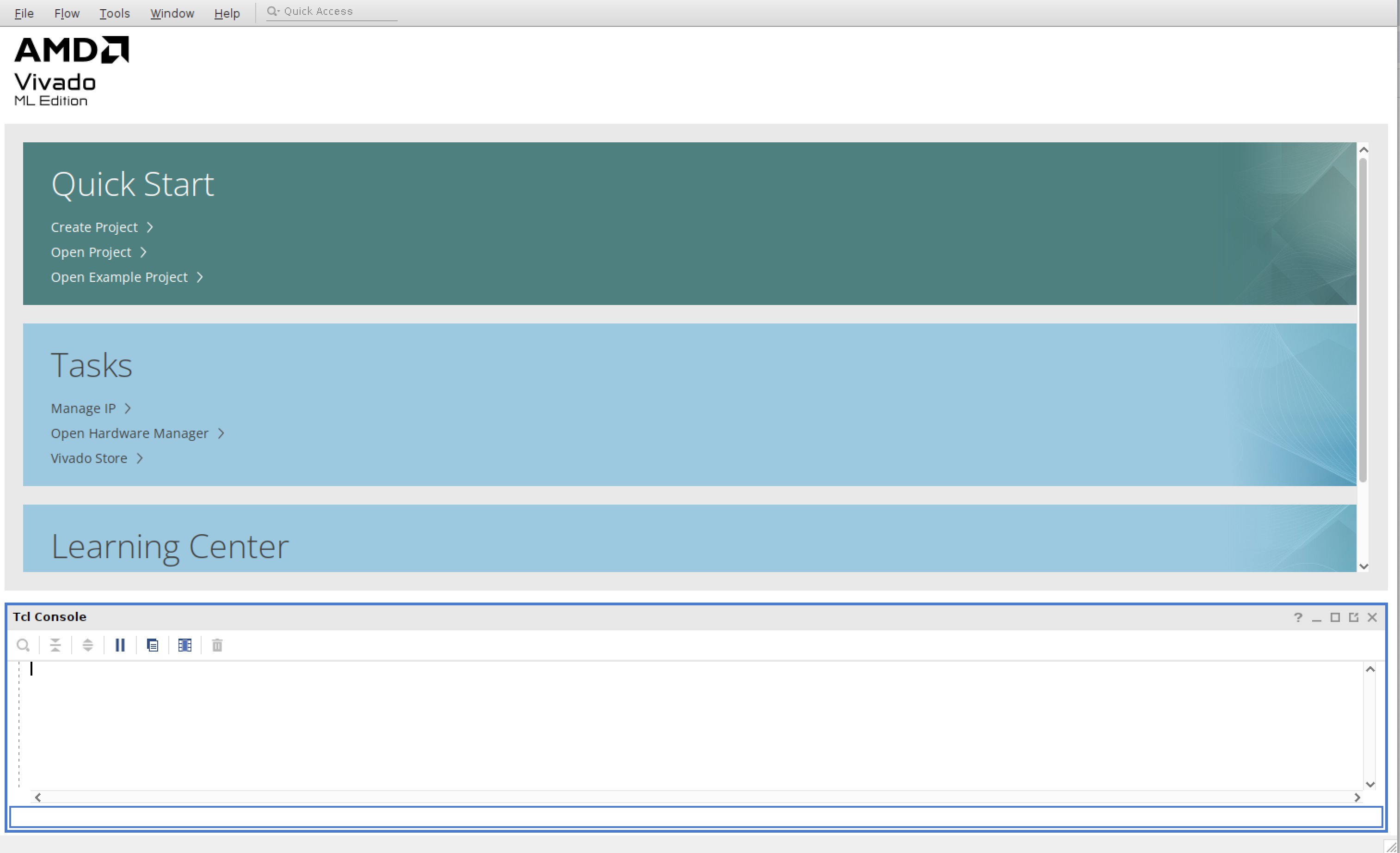
The Vivado initial console window will open as shown below:

The bottom of this window is the “TCL Console” where you can enter TCL commands as you did in an earlier tutorial.
Pre-Synthesis Schematic
Begin by executing the initial read_verilog command to perform HDL analysis.
read_verilog -sv binary_adder.sv
Executing this command will create new window panes in the Vivado tool
Next, run the synth_design command to perform RTL elaboration (but not full synthesis) on the design.
synth_design -top binary_adder -rtl -rtl_skip_mlo -part xc7a35tcpg236-1 -verbose
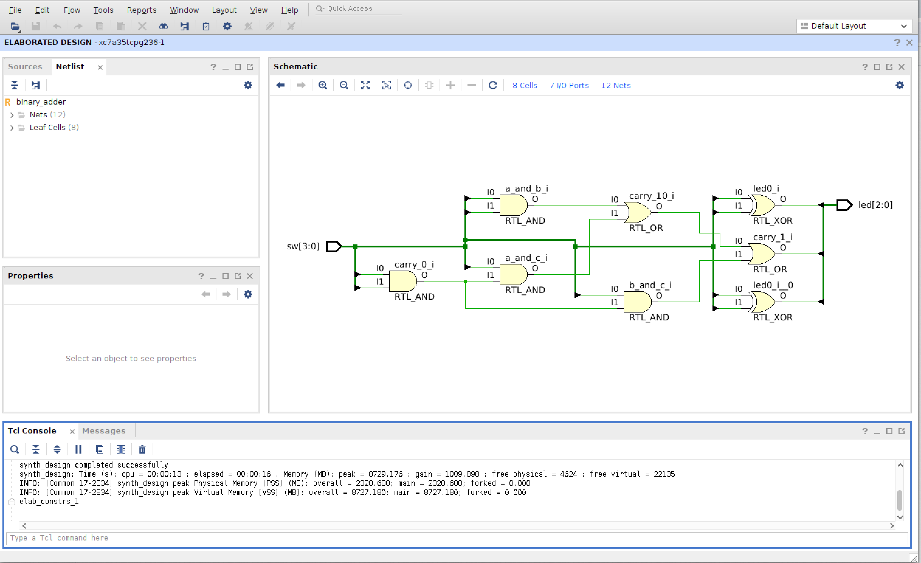
This will perform RTL elaboration and display the structural connectivity of the design in the “Schematic” window as shown below.

It is often more convenient to create a ‘.tcl’ script that runs all of these commands at once in batch mode. You can create a .tcl file with the two commands above and run the following command to generate the schematic:
vivado -source synth_schematic.tcl -log synth_schematic.log -nojournal -notrace
Post-Synthesis Schematic
To generate a schematic of the post-synthesis design, first synthesize the design as described in the command-line synthesis tutorial. You should have a ‘.dcp’ file after successfully completing this step. Run Vivado in GUI mode as described above.
In the Vivado tcl console, execute the following command:
open_checkpoint binary_adder_synth.dcp
This will bring up a window with the device ‘Design’ and several panes that contain information about your design. The window should look something like:

The ‘Device’ window on the right provides an overview of the FPGA resources that the design will be mapped to. In the top-left is the ‘Netlist’ window that summarizes the details of the design (internal nets and cells). The bottom left window provides a summary of the netlist.
To open the post-synthesis schematic, do the following:
- Select the ‘Binary Adder’ in the ‘Netlist’ Pane.
- Right Click and select “Schematic”