The Vivado tools can be used to query the layout of your logic implementation on the FPGA.
This tutorial will describe how you can view the internals of the FPGA mapped with your design.
This tutorial is written with your lab03 logic_functions.sv design.
Before proceeding with this tutorial, you need to have fully implemented your design and have a file named `logic_functions.dcp.
Open Vivado with Design Checkpoint
Open the vivado tool in GUI mode:
% vivado &
In the Vivado tcl console, execute the following command:
open_checkpoint logic_functions.dcp
This will bring up a window with the device ‘Design’ and several panes that contain information about your design. The window should look something like:

This image shows the internals of the FPGA resources and your design resources mapped onto the FPGA. Since your design is relatively small, your design resources are not easiliy noticable.
Viewing Design Resources
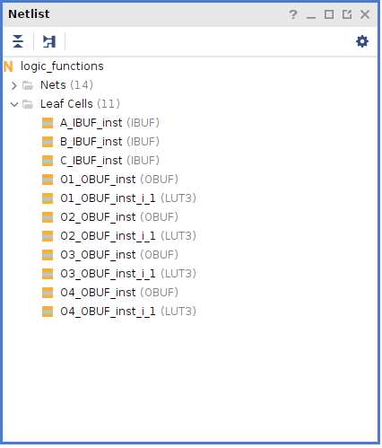
To view the location of design resources, expand the “Leaf Cells” line within the ‘Netlist’ Pane. This will list all of the design resources mapped to the FPGA.

Select one of the ‘LUT’ resources in your list.
After you select a resource, click ‘Auto-fit Selection’ button: ![]() .
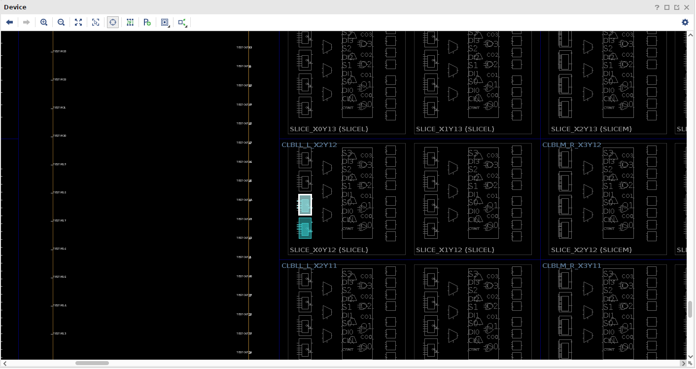
The design viewer will then zoom into the area of the device that contains the resource with the resource highlighted.
An example looks like this:
.
The design viewer will then zoom into the area of the device that contains the resource with the resource highlighted.
An example looks like this:

By default, this view only shows the cell resources and not the net resources.
Enable the viewing of the net resources by clicking on the ‘Routing Resources’ button: ![]() .
.
You can zoom in and out of the design with the following buttons:
- Full Zoom:

- Zoom Selection:

- Zoom In:

- Zoom Out:

You can also view specific nets within the design.
Select a net in the ‘Netlist’ Pane under the ‘Nets’ line.
After selecting the net, Click the Zoom Selection button![]() .
.