Table of Contents
Resources
- BitmapToVga module
- clk_generator module
VGA Video
You have been given a module, BitmapToVga, that internally stores a Bitmap image, and continually sends the image out over the VGA port on the board as 640x480 video.
Internally, the bitmap image is 320x240 pixels. For each pixel in the image, 3 bits are stored: 1 bit for red, 1 bit for green, and 1 bit for blue. For example, a pixel set to 3’b000 will display black, 3’b111 white, 3’b100 red, 3’b010 green, 3’b001 blue, 3’b101 magenta, 3’b011 cyan and 3’b110 for yellow. Upon power-on, the bitmap image will be all black, but using the inputs to the BitmapToVga module, you can change the color values of the 320x240 pixels, one at a time.
Note: Although the VGA output is 640x480, the bitmap is only 320x240 pixels, because the limited memory on the FPGA would make it difficult to store a full 640x480 image. The BitmapToVga module automatically scales up the image to the 640x480 resolution before sending it to the display.
| Module Name = BitmapToVga | |||
|---|---|---|---|
| Port Name | Direction | Width | Description |
| clk | Input | 1 | 100 MHz Clock |
| clk_vga | Input | 1 | 25 MHz Clock for 640x480 VGA Display |
| reset | Input | 1 | Active-high reset |
| x | Input | 9 | x-Coordinate of pixel to modify (0..319) |
| y | Input | 8 | y-Coordinate of pixel to modify (0..239) |
| color | Input | 3 | Color of pixel. [2]=red, [1]=green, [0]=blue |
| wr_en | Input | 1 | Write enable – set to 1 to enable writing to the bitmap image |
| VGA_R | Output | 4 | VGA Red (to external connection) |
| VGA_G | Output | 4 | VGA Green (to external connection) |
| VGA_B | Output | 4 | VGA Blue (to external connection) |
| VGA_hsync | Output | 1 | VGA Horizontal Sync (to external connection) |
| VGA_vsync | Output | 1 | VGA Vertical Sync (to external connection) |
Drawing Pixels
The BitmapToVga module has inputs that let you change the value of the pixels in the bitmap image, allowing you to draw things on the VGA monitor.
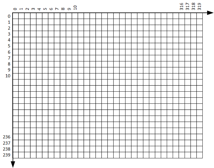
The (x,y) layout of the bitmap is shown below:
The following waveform example demonstrates writing the (35, 40) pixel to red, the (34, 41) pixel to green and the (100, 2) pixel to yellow.
![]()
VGA Clock
The BitmapToVga requires a 25MHz clock. This is because the 640x480 VGA standard requires that pixels be sent at a rate of ~25MHz.
You have been given the clk_generator module that uses special circuity on the FPGA (a Phase-Locked Loop (PLL), https://en.wikipedia.org/wiki/Phase-locked_loop) to derive a new clock based on the input 100MHz clock.
| Module Name = clk_generator | |||
|---|---|---|---|
| Port Name | Direction | Width | Description |
| clk_in_100 | Input | 1 | 100 MHz Input Clock |
| clk_vga | Output | 1 | 25 MHz Generated Clock |
| clk_100 | Output | 1 | 100 MHz Generated Clock |
Note: The clk_generator module also contains a 100MHz clock output. The reason for this is because once you input your 100MHz clock into the PLL circuity, the tools will not let you use it elsewhere in your design. Thus you will need to use the clk_100 output of this module to clock the rest of your design.