Table of Contents
The purpose of this laboratory is to design a circuit for generating the VGA synchronization signals. You will use this controller to create a “color bar” on the display. You will also use this controller in future labs to display other things on a VGA compatible display.
The average time to complete this lab is 5.1 hours.
Learning Outcomes
- Understand the timing signals required to drive a VGA display
- Understand how to create colors on the VGA display
- Create a reusable digital circuit for controlling the timing of a VGA display
Preliminary
In order to design a VGA controller, it is necessary to understand how the VGA display works and the timing of the synchronization signals required to drive the VGA display. This preliminary section of the lab will guide you through this information to prepare you for designing the VGA controller. Begin by reviewing the VGA Port section of the Basys3 Reference Manual to learn more about how the VGA is wired on the Basys3 board.
There are a number of figures and diagrams in this section that are helpful. In particular, look for the table in the manual that shows the exact pixel counts for the front porch, sync pulse, back porch, and visible area. For 640×480 at 60 Hz (with a 25 MHz pixel clock), you will see the following breakdown:
- Horizontal: 640 (display) + 16 (front porch) + 96 (sync pulse) + 48 (back porch) = 800
- Vertical: 480 (display) + 10 (front porch) + 2 (sync pulse) + 29 (back porch) = 521
These values tell you exactly when h_sync and v_sync must go low (their active phase). Although many references online show various VGA timings, you must use the Basys3’s official table for 640×480 at 60 Hz. Slight mismatches can cause display instability or no image at all.
After reviewing this section, answer the following questions in the lab report.
What pin number on the VGA connector is the HS signal connected to?
How many different color levels can be created for each of the three color VGA signals?
What is the range in voltage of the color signal (fully off to fully on)?
The voltage of each color signal is determined by a voltage divider between the 75 ohm termination resistance of the VGA display and the resistor divider circuit connected to the FPGA. What is the voltage on the RED VGA color signal when RED0=0, RED1=0, RED2=1, and RED3=1?
What values on the RED0, RED1, RED2, RED3, GRN0, GRN1, GRN2, GRN3, BLU0, BLU1, BLU2, and BLU3 signals are needed to generate the “full intensity” red color (i.e., provide the maximum analog voltage on the RED signal and the minimum analog voltage on the GREEN and BLUE signals)?
What does CRT stand for?
The VGA display requires two synchronization signals, Horizontal Sync (HS) and Vertical Sync (VS), to drive the display. The timing of these signals is critical to the proper operation of the VGA display.
What is the frequency of the pixel clock for the 640x480 VGA resolution?
What is the period of the horizontal sync signal (HS) for the 640x480 resolution?
What is the period of the vertical sync signal (VS) for the 640x480 resolution?
During the scan of one horizontal row, 640 pixels are displayed. However, additional time is needed during the horizontal scan for retracing. How many pixel clocks are needed during each horizontal sync for this retracing (i.e. how many pixel clocks are used when no pixel is displayed in a horizontal scan)?
How many frames per second are generated with this timing?
How many lines are NOT displayed during a full frame (i.e. lines that are blanked during a vertical retrace)?
How many pixel clocks is the horizontal sync signal low during a horizontal sync pulse?
How many pixel clocks is the vertical sync signal low during a vertical sync pulse?
Assuming the ‘display’ phase occurs first, determine the ordering of the four phases of a sync signal.
Do NOT proceed to the design until you have answered the questions above. If you are not able to answer these questions it will be difficult for you to complete the timing controller.
Exercises
Make sure to merge in any changes from the startercode before starting the lab.
Here is an overview of the exercises you will complete in this lab:
- Exercise 1: VGA Timing Controller: Before worrying about the pixel colors, we first need to create the timing signals for the VGA display. Without correct timing signals, the monitor will not be able to synchronize with your circuit and you will not see any image on the display. In this exercise, you will create a VGA timing controller that generates the correct timing signals for the VGA display.
- Exercise 2: VGA Timing Controller Testbench: After creating your VGA timing controller, you will test it with a provided test bench.
- Exercise 3: Top-level Design: You will create a top-level design that instantiates your VGA timing controller and generates the pixel color signals for the VGA display. In this lab, the colors will simply be one of black, white, a color determined by the switches, or a vertical color bar. In future labs, you will create more interesting images on the VGA display.
- Exercise 4: Top-level Design Simulation: You will create a tcl simulation to verify your design.
- Exercise 5: Synthesis, Implementation, and Download: You will verify the correct operation on the board.
Exercise 1: VGA Timing Controller
Create a new file named vga_timing/vga_timing.sv that contains the timing generator for your VGA controller.
Create a module with the following input ports, and output ports:
| Port Name | Direction | Width | Function |
|---|---|---|---|
| clk | Input | 1 | 100 MHz Clock signal |
| rst | Input | 1 | Synchronous reset |
| h_sync | Output | 1 | Low asserted horizontal sync VGA signal |
| v_sync | Output | 1 | Low asserted vertical sync VGA signal |
| pixel_x | Output | 10 | Column of the current VGA pixel |
| pixel_y | Output | 10 | Row of the current VGA pixel |
| last_column | Output | 1 | The current pixel_x correspond to the last visible column |
| last_row | Output | 1 | The current pixel_y corresponds to the last visible row |
| blank | Output | 1 | The current pixel is part of a horizontal or vertical retrace and that the output color must be blanked. |
After you have created your module ports, create your VGA timing controller as described below.
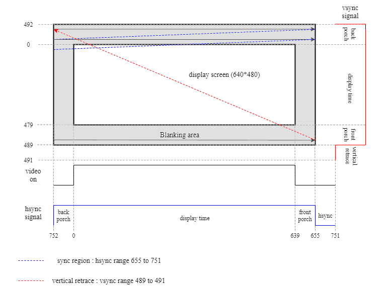
Also, use the following figure as reference for how these signals correspond with their respective locations on the screen.
Note: Coding standard rule S19 requires that only one signal can be assigned in a always_ff block.
You will be creating multiple registers in the discussion below and need to make sure that each register is in a separate always_ff block.
Notice that the values wrap (i.e. 0 does not start at the very end or beginning, but rather at the start of the display region):
Clock Divider Counter
For the 640x480 VGA resolution that we are implementing, the pixels change at a frequency of 25 MHz (this is called the pixel clock). This is one-fourth the frequency of the 100 MHz clock that is provided with the Basys3 board. You will need to create a signal that is asserted every fourth clock cycle of the 100 MHz clock to be used by the VGA timing circuitry.
- Create a signal named
pixel_enthat can be used by internal synchronous circuitry to “enable” the updating of VGA timing counters. Write the necessary RTL code so that this signal goes high every fourth clock cycle (i.e., three cycles of 0 followed by one cycle of 1, then repeat). This can be done by creating a counter with sequential logic, and then using combinational logic to assertpixel_enwhen the counter reaches a certain value.
Horizontal Pixel Counter
The pixel_x output of your module should indicate the current column of the VGA display that is being processed.
This should be a counter that counts from 0 to 799 (640 displayed pixels, 16 front porch pixels, 48 back porch pixels, and 96 “pulse” pixels). Remember, when pixel_x 0, it indicates that the first visible pixel is being displayed, when 639, the last visible pixel is being displayed, and when greater than 639, it indicates a column associated with the retrace phase.
Make sure your counter resets to zero when rst is asserted, and increments at a rate of 25 MHz (i.e, only increment when pixel_en is high).
Like all counters, it should be implemented with sequential logic in an always_ff block.
The last_column output signal indicates when the current column being processed is the last visible column (i.e., when pixel_x is 639). Make sure you use combinational logic to generate this, as you want it to be high during the same cycle that pixel_x is 639, not the cycle after.
Vertical Pixel Counter
Likewise, the pixel_y output of your module should indicate the current row of the VGA display that is being processed.
This should also be a counter, and it should count from 0 to 520.
When this counter is 0, it indicates that the first visible line is being displayed, and when 479, the last visible line is displayed.
The pixel_y counter should increment when at the end of each horizontal line (i.e., when pixel_x reaches its maximum value), and pixel_en is high (i.e., at a rate of 25 MHz).
Make sure to use combinational logic to generate the last_row output signal (i.e., when pixel_y is 479).
Timing Signals
The pixel_x and pixel_y counters that you created above will help a parent module determine exactly which pixel is being processed at any given time; however, the VGA display does not use these counters directly.
As you learned in the preliminary section, the VGA display uses the horizontal and vertical sync signals (hsync and v_sync).
We need to generate these outputs.
Remember that for VGA on the Basys3 board, h_sync and v_sync are active low.
As described in the Basys3 Reference Manual, each timing signal has four phases:
- Display Phase (signal=1): during this phase the image is displayed on the screen.
- Front Porch Phase (signal=1): a brief waiting period after the display phase ends.
- Pulse Phase (signal=0): the sync signal is asserted, triggering the retrace.
- Back Porch Phase (signal=1): settling time after the sync pulse before the next display phase begins.
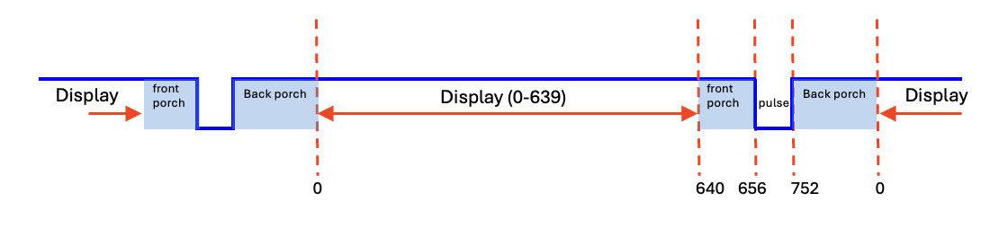
For example, here is a timing diagram that shows the horizontal timing signals and how they correspond to the pixel_x counter:
You will use the pixel_x counter to determine the h_sync signal and the pixel_y counter to determine the v_sync signal.
The tables below summarizes each phase and the corresponding counter values:
| Phase | Horizontal Counter | Pixel Clocks | h_sync |
|---|---|---|---|
| Display | 0-639 | 640 | 1 |
| Front Porch | 640-655 | 16 | 1 |
| Pulse | 656-751 | 96 | 0 |
| Back Porch | 752-799 | 48 | 1 |
| Phase | Vertical Counter | Lines | v_sync |
|---|---|---|---|
| Display | 0-479 | 480 | 1 |
| Front Porch | 480-489 | 10 | 1 |
| Pulse | 490-491 | 2 | 0 |
| Back Porch | 492-520 | 29 | 1 |
Create combinational logic to generate the h_sync and v_sync signals based on the current values of the pixel_x and pixel_y counters.
Blank Signal
The blank output signal should be high when the current pixel is part of a horizontal or vertical retrace (i.e., during the front porch, pulse, and back porch phases).
This will be a helpful signal for the parent module to know when valid
Include the file vga_timing/vga_timing.sv in your repository.
Exercise 2: VGA Timing Controller Testbench
Like the previous labs, a testbench, tb.sv, has been provided for you to test your VGA timing controller.
This testbench is very picky about timing and will complain if there are any timing problems.
Run the testbench and make sure your VGA timing controller is functioning correctly.
If you see a large number of error messages, you may want to run the simulation in the Vivado GUI where you can manually step through the simulation time to help debug your design.
Use make sim_tb_gui as described in the Simulation (Testbench) Section of the Common Makefile Documentation to open the Vivado simulator with your testbench loaded.
Begin by simulating for only a few microseconds.
If you have problems with your horizontal timing, you will see messages in a short amount of time.
After resolving any of your horizontal timing problems, simulate for a longer period of time to see if your vertical timing is correct.
Continue simulating and debugging until you do not see any error messages from the testbench.
You will need to simulate for a relatively long period of time until the “simulation done” message appears.
Make sure the testbench (make sim_tb) runs without any errors before proceeding.
Exercise 3: Top-level Design
Create a new file named vga_top/vga_top.sv that contains the logic for generating the pixel colors on the VGA display.
Define a module named vga_top and provide the following top-level ports:
| Port Name | Direction | Width | Function |
|---|---|---|---|
| clk | Input | 1 | 100 MHz Clock signal |
| btnd | Input | 1 | Asynchronous reset |
| btnc | Input | 1 | Display color from switches |
| btnl | Input | 1 | Display White |
| btnr | Input | 1 | Display Black |
| sw | Input | 12 | Switches to determine color to display |
| Hsync | Output | 1 | Horizontal synchronization signal |
| Vsync | Output | 1 | Vertical synchronization signal |
| vgaRed | Output | 4 | Red color signal |
| vgaGreen | Output | 4 | Green color signal |
| vgaBlue | Output | 4 | Blue color signal |
Here is what your top-level design should do:
- Instance your VGA timing controller.
- Connect the
clksignal. - Use
btndas the reset. last_rowandlast_columnwon’t be used in this lab, so you can leave them unconnected.- Create an internal signal for the
blankoutput of the VGA timing controller. - The connections for the other ports are described in the next steps.
- Connect the
-
The next step is to write the logic to generate the pixel colors for the VGA display. This should be combinational logic that determines the color of each pixel based on the current
pixel_xandpixel_yvalues from the VGA timing controller, as well as the button and switch inputs to your top-level design.Do not assign directly to the
vgaRed,vgaGreen, andvgaBlueoutputs of your top-level design, but instead create internal signals for the red, green, and blue colors. The example code below uses the namesred_disp,green_disp, andblue_disp, but you can use any names you prefer. Make sure these are the correct bit width (4 bits for each color).Interesting objects, images, animation, and user interfaces can be displayed by creating custom logic based on the x,y location of the VGA display. For example, this code creates a display where the left half of the screen is red and the right half of the screen is green:
assign red_disp   = (pixel_x < 320)  ? 4'b1111 : 4'b0000;
assign green_disp = (pixel_x >= 320) ? 4'b1111 : 4'b0000;
assign blue_disp  = 4'b0000;
You should implement the following logic to determine the color of each pixel, in priority order:
- When the
blanksignal from the VGA timing controller is high, the color must be black (i.e., Red=0000, Green=0000, and Blue=0000). - When
btnris pressed, display the color black on the display. - When
btnlis pressed, display the color white on the display. - When button
btncis pressed, display a single uniform color on the screen where the color is determined by the twelve switches (Red=SW[11:8], Green=SW[7:4], and Blue=SW[3:0]). - When no buttons are pressed, create a vertical “color bar” test pattern. Color bars were often used in analog televisions to test the television, color, and brightness and the television transmission. Your test pattern should have 8 vertical colors bars, each 640/8 = 80 pixels wide, that cover the entire height of the screen. The colors of the bars should be as follows (from left to right):
- Black: RGB=0,0,0
- Blue: RGB=0,0,f
- Green: RGB=0,f,0
- Cyan: RGB=0,f,f
- Red: RGB=f,0,0
- Magenta: RGB=f,0,f
- Yellow: RGB=f,f,0
- White: RGB=f,f,f
You are free to design the combinational logic as you see fit. However, you may consider creating an intermediate signals for the vertical color bar pattern and then using a multiplexing logic to select between the vertical color bar, the switch-based color, white, and black based on the button inputs.
- When the
-
The combinational logic you created in the previous step will generate the correct colors for each pixel, but these signals may contain temporary glitches when the signals change values. In addition, the
h_syncandv_syncsignals from your VGA timing controller were also generated with combinational logic and may also contain glitches.It is important that these glitches are not transmitted to the VGA display. Glitches on the VGA timing signals may lead to improper VGA synchronization. Glitches on the VGA colors may generate improper colors on the display.
To remove the glitches, make sure your color logic, as well as the
h_syncandv_syncsignals from the VGA timing controller, are all registered (i.e. passed through flip-flops) before being sent to the VGA display. The figure below shows the circuit structure:
You should now have logic to drive all of the outputs of your top-level design.
Reset Behavior
Based on how you created your design, while btnd is pressed, the VGA timing controller should be held in reset.
This means it will not generate any VGA timing signals and the VGA monitor will temporarily lose synchronization with your circuit.
You may see a message on the monitor indicating that it is not receiving a signal.
Note that this is different that just sending a black color to the monitor, which would still allow the monitor to synchronize with your circuit (since the timing signals are still being generated).
Exercise 4: Top-level Design Simulation
Once you have created your top-level design, create a tcl simulation script (sim.tcl) to simulate the behavior of your top-level design.
Include the file vga_top/sim.tcl in your repository.
Your tcl simulation script should do the following:
- Create a free running clock
- Set default values for all the inputs (all buttons off, switches to 0)
- Issue the reset for a few clock cycles
- Run the simulation for ~10 vertial lines (4x800x10 clocks) so you can make sure the colors are correct. Make sure that the colors are ‘black’ during the blanking period.
- Set ‘btnl’ to high and simulate for ~10 lines to make sure the colors are white
- Set ‘btnr’ to high (and ‘btnl’ to low) and simulate for ~10 lines to make sure the colors are black
- Set ‘btnc’ to high (and ‘btnr’ and ‘btnl’ to low) and simulate for ~10 lines to make sure the colors are the same as the switches
- Run this for at least 2 different switch settings.
Look over your simulation waveforms to verify that your top-level design is functioning correctly. Check that the colors are correct based on the button and switch settings, and that the colors are black during the blanking periods. Take a screenshot of the full simulation waveform and save it.
Include the file vga_top/sim.png in your repository.
Exercise 5: Synthesis, Implementation, and Download
-
Create a
basys3.xdcfile that contains pin location definitions for each of your I/O ports.Include the file
vga_top/basys3.xdcin your repository. -
Run synthesis. Carefully review the synthesis log to make sure there are no warnings.
How many total flip-flops (FDCE or FDRE) cells are used by the design?
How many total LUT resources are used by the design? (add up all the LUT* resources)
How many total IBUF and OBUF resources do you have in the design?
-
Run implementation.
-
Download the bitstream to the Basys3 board and verify that the VGA controller is functioning as expected.
-
Review the
utilization.rptfile to answer the following questions.How many ‘Slice LUTs’ are used by your design?
How many ‘Slice Registers’ are used by your design?
-
Review the
timing.rptfile to answer the following questions.What is the Worst Negative Slack or ‘WNS’ of your design?
How many TNS total Endpoints are there in your design?
-
Open your implemented design in Vivado, find the flip-flops associated with the
pixel_xcounter and zoom into the device implementation that shows these flip-flops. Make sure the routing is shown and take a screenshot of the resources used to create this counter.Include the file
vga_top/fpga.pngin your repository.
Final Pass-Off
Refer to the passoff tutorial for the passoff process.
- See
required_filesin the passoff script. - Makefile rules that must work correctly and be free from errors and warnings:
Makefile:cleanvga_timing/Makefile:sim_tbvga_top/Makefile:synth,implement
Answer the final two questions in your laboratory report:
How many hours did you work on the lab?
Provide any suggestions for improving this lab in the future