Table of Contents
In this laboratory you will create and test an asynchronous receiver.
The average time to complete this lab is 5 hours.
Learning Outcomes
- Strengthen your understanding and skill in designing FSMs
- Implement an asynchronous receiver
Preliminary
Designing the receiver is very similar to the design of a transmitter and your receiver module will have many of the components that your transmitter module had. A discussion of the receiver and the differences between the transmitter are described in Section 28.4 of the textbook. The instructions for the receiver are less detailed than the transmitter so you will need to do more of the design work on your own. In particular, you will need to create the state machine for the receiver from scratch.
Like the transmitter, the default mode of the receiver is to receive data at a baud rate of 19200 with ODD parity, 8 bits of data, and one stop bit.
Using a 100 MHz clock, how many clock cycles are in half of a bit period for a baud rate of 19200? (see Figure 28.15)
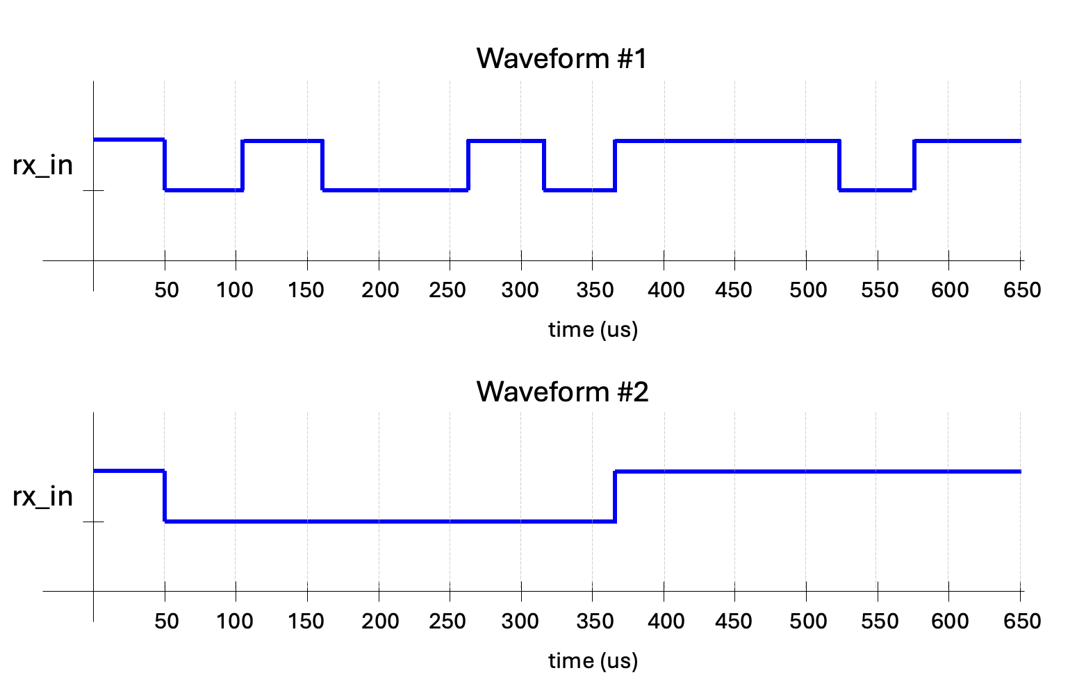
In the first waveform shown below, what is the 8-bit sequence recevied by the receiver with a baud rate of 19200?
Is the parity bit of the first waveform indicating a successful transmission?
In the second waveform shown below, what is the 8-bit sequence received by the receiver with a baud rate of 19200?
Is the parity bit of the second waveform indicating a successful transmission?
Exercises
Exercise #1 - Asynchronous Receiver Module
Begin your laboratory assignment by creating a receiver module in a file named rx.sv that has the following parameters and ports:
| Parameter | Default | Function |
|---|---|---|
| CLK_FREQUENCY | 100_000_000 | Specifies the frequency of the clock in Hz |
| BAUD_RATE | 19_200 | Determine the baud rate of the transmitter |
| Module Name: rx | |||
|---|---|---|---|
| Port Name | Direction | Width | Function |
| clk | Input | 1 | 100 MHz System Clock |
| rst | Input | 1 | System reset active high |
| Sin | Input | 1 | Receiver serial input signal |
| Receive | Output | 1 | Indicates that a byte is ready to send on the Dout pins. (Receive serves as REQ in Figure 28.7.) |
| ReceiveAck | Input | 1 | Indicates that the byte on the Dout pins has been received. (ReceiveAck serves as ACK in Figure 28.7.) |
| Dout | Output | 8 | 8-bit data received by the module. Valid when Receive is high. |
| parityErr | Output | 1 | Indicates that there was a parity error. Valid when Receive is high. |
Next, complete the full design of the receiver. Although there are many ways to build your receiver, your module will need the following components:
- Baud timer
- Bit counter
- Shift register
- Parity checker
- Finite State Machine Each of these are described below.
Baud Timer
This is very similar to your timer in the transmitter except it needs to be able to tell you when a whole bit time has passed as well as when a half bit time has passed. Like the transmitter timer, the baud timer maximum count value should be based on the module parameters. Both are needed at some point in your state machine’s operation. One way to implement this is to simply add a second output to the timer to signify when it has reached its half-count. It need not roll over when it reaches its half-count – it can simply raise this second output and keep counting until it reaches the full count.
Bit counter
Like the transmitter, you will need a bit counter that keeps track of the bits received.
Shift Register
The purpose of the shift register is to collect the serially received bits as they come in. Design the shift register so that it resets with the global reset signal. As described in the text, the shift register should sample the serial input in the middle of each bit period (this is the responsibility of the state machine). You will need to store all 8 data bits plus the parity bit so you can check the parity. You will only output the 8 data bits on the ‘Dout’ pins.
Parity Checker
Once you have shifted all bits into the shift register, you should check that the parity bit is correct (ODD parity). If this is not true, you should raise the ‘parityErr’ signal.
The ‘parityErr’ signal can be implemented with combinational logic that computes the parity on incoming data in the shift register and tests to see if it does not match the expected parity (ODD in this case). The error signal will thus transition as things are shifted into the shift register, and it will only be accurate once you have shifted in the last bit. That is OK – the host logic will only look at the parityErr signal when Receive == 1.
Finite State Machine
Unlike the transmitter, the receiver state machine is not given to you, and you will need to design it from scratch. We suggest you pattern it somewhat after the transmitter state machine. A few guidelines for this state machine are given below.
‘INIT’ STATE: When in an ‘IDLE’ state, the receiver will constantly be watching the “Sin” signal to go low to indicate the start bit. It is possible that the input signal from the remote transmitter is low when the receiver first starts up. This could be for several reasons including: the transmitter is powered off and the transmit signal is low, the transmitter is permanently low due to some sort of fault, or the transmitter is designed poorly such that the transmit signal starts out low before being initialized. Your receiver must be designed with some sort of initialization state to ignore any initial low signal on the “Sin” input before proceeding to the ‘IDLE’ state. Without this initialization state, your receiver will continuously see the “Sin” signal as low and receive data that is not valid. Include an initialization state to your state machine that waits for the “Sin” signal to go high before transitioning to an ‘IDLE’ state. The purpose of this state is to prevent the receiver from starting the state machine sequence until the serial input is initially high.
Input Sampling: Unlike the transmitter where you shifted the data out after the end of each baud period, you will need to sample the serial input in the middle of each bit period. Design your state machine to sample data (i.e., shift the shift register) in the middle of the baud period rather than the end.
Handshaking: Your state machine will need to implement a handshaking protocol with the outer module using the ReceiveAck and Receive signals.
Once the full transmission has completed (i.e., the stop bit, all 8 data bits, the parity bit and the stop bit have been received), enter a ‘WAIT’ state to indicate that the transmission is complete.
Assert the Receive signal when you enter this state to indicate to the outer module that the receiver has a byte to hand off.
Wait in this state until the ‘ReceiveAck’ signal is asserted by the outer module to indicate that the byte has been accepted.
Exercise #2 - Receiver Simulation
After creating your ‘rx’ module, create a Tcl file named sim_rx.tcl and simulate your receiver module.
Your tcl file should include the following:
- Run the simulation for 100ns without setting any values
- Create a 100 MHz oscillating clock and run for a few clock cycles
- Set the reset to ‘1’ and default values for all inputs and run for a few clock cycles
- Deassert the reset signal and run for a few clock cycles
- Emulate the transmission of the following byte: 0x41 (ASCII ‘A’) using a baud rate of 19,200 and correct ODD parity.
- Run for at least 100 us after the end of the serial transmission
- Assert ‘ReceiveAck’ and run for 10 us
- Emulate the transmission of the following byte: 0x5e (ASCII ‘^’) using a baud rate of 19,200 and incorrect ODD parity (i.e., generate a parity signal that is incorrect and should cause a parity error output).
After completing the simulation, take a screenshot of the waveform and name the file sim_rx.png
After simulating your module and verifying it operates with the Tcl script, you will need to test your receiver with a testbench.
The testbench file is named tb_rx.sv and is located as part of the starter code in your lab repository.
Begin by testing the decoder interactively in GUI mode with this testbench to resolve syntax and behavioral problems in your design.
Once you have resolved these issues, create a Makefile rule named sim_rx_tb that will run the simulation of your seven-segment controller with the testbench.
This rule should generate a log file named sim_rx_tb.log.
Make sure that your testbench simulates without any errors.
How many characters are sent by the testbench?
What is the sixth character transmitted in the testbench?
What is the time in nano seconds in which the simulation ends?
Exercise #3 - Top-level Design
In this exercise you are going design the top-level circuit to test your receiver module.
Make a new top-level module in a file named rx_top.sv with the following parameters and ports:
| Parameter | Default | Function |
|---|---|---|
| CLK_FREQUENCY | 100_000_000 | Specifies the frequency of the clock in Hz |
| BAUD_RATE | 19_200 | Determine the baud rate of the transmitter |
| REFRESH_RATE | 19_200 | Determine the seven segment display refresh time |
| Module Name: rx_top | |||
|---|---|---|---|
| Port Name | Direction | Width | Function |
| clk | Input | 1 | 100 MHz System Clock |
| btnd | Input | 1 | Reset signal |
| rx_in | Input | 1 | Input receiver signal |
| parityErr | Output | 1 | Parity error signal, displays to led[15] |
| segment | Output | 8 | Cathode signals for seven-segment display |
| anode | Output | 4 | Anode signals for each of the four display digits |
| rx_debug | Output | 1 | RX Debug signal for visualizing rx_in, displays to led[0] |
Create the following components as part of your top-level module.
Synchronizers
A synchronizer is needed for the two input signals ‘btnd’ and ‘rx_in’. Create a two flip-flop synchronizer between ‘btnd’ and your internal reset signal. Also, create a two flip-flop synchronizer for ‘rx_in’.
Instance rx module
Instance your ‘rx’ module and make the following connections to your ‘rx’ module:
- Connect the top-level
clkto theclkinput of your rx module - Connect the synchronized reset signal from
btndto therstinput of your rx module - Connect the synchronized
rx_insignal to theSininput of your rx module - Connect the inverted value of
rx_into your top-levelrx_debugoutput port
Connections to the other ports will be described below.
Handshaking Signals and Data Registers
You will need to create additional logic to interact with the handshaking protocol of the receiver and to store the results of the received data and parity error status into registers.
- Create an ack signal and assign it directly to the Receive output from the rx module. This ensures the acknowledgment of the received data byte occurs in the same cycle that Receive goes high. You’ll then connect this ack signal back into the ReceiveAck input, using it to trigger loading the received data into your internal registers.
- Create an 8-bit register to store the value received from the ‘rx’ module. Use the ‘acknowledge’ signal to load this register from the data coming from the ‘rx’ module.
- Create an 8-bit counter that increments the count value every time a new character is received. Use the ‘acknowledge’ signal to increment this counter.
- Create a one-bit register to store the value of the ‘parity error’ from the ‘rx’ module. Use the ‘acknowledge’ signal to load this register. Attach the output of this register to the ‘parityErr’ output port of the top-level module.
Seven Segment Controller
Instance your seven-segment display controller and connect the inputs to your controller as follows:
- Attach the 8-bit data register you created above to the bottom 8 bits of the data input of the seven-segment controller.
- Attach the 8-bit character counter register to the upper 8 bits of the data input.
- Display all four digits.
- Enable the third digit point so that there is a digit point between the lower two digits and the upper two digits.
- Attach the anode and segment signals of the controller to the top-level outputs of the top-level module
NOTE: To use your seven_segment4.sv module (and any other modules from previous projects you will be using here) you need to reference the module in your tcl and makefile using a relative path: ../lab07/seven_segment4.sv
and NOT by copying and pasting the module into each project.
Once you have completed your top-level module, simulate your top-level module with a ‘tcl’ script to make sure that the buttons are properly hooked up.
Name your simulation script sim_rx_top.tcl and perform the same operations in your top-level script that you performed for your receiver module simulation script.
You may want to copy your other tcl script and adapt the signal names for the top-level.
When you have completed the simulation, create a screenshot of the simulation waveform and save it as sim_rx_top.png.
Exercise #4 - Implementation
Once you are satisfied with your top-level circuit’s behavior, create a .xdc file that contains pin location definitions for each of your I/O ports. Add .xdc entries for the ‘clk’, ‘btnd’, ‘segment’, and ‘anode’ top-level ports. Add the other top-level ports as follows:
rx_in: Attach the ‘rx_in’ signal to the Basys3 board’s USB UART receiver pinB18(RsRx)rx_debug: Attach the ‘rx_debug’ signal to the Basys3 board’s LED 0parity_err: Attach the ‘parityErr’ signal to the Basys3 board’s LED 15
Create a Makefile rule named synth that runs the synthesis script and generates a log named synthesis.log and a ‘.dcp’ file named rx_top_synth.dcp.
Carefully review the synthesis log to make sure there are no Warnings.
How many FDxE cells are used by the design?
How many total LUT resources are used by the design? (add up all the LUT* resources)
How many total IBUF and OBUF resources do you have in the design?
After successfully synthesizing your design, begin the implementation process by creating a Makefile rule named implement that runs an implementation tcl script.
This rule should generate a log named implement.log, a ‘.dcp’ file named rx_top.dcp, a ‘.bit’ file named rx_top.bit, a utilization report named utilization.rpt, and a timing report named timing.rpt.
Review the ‘utilization.rpt’ file to answer the following questions.
How many ‘Slice LUTs’ are used by your design?
How many ‘Slice Registers’ are used by your design?
Review the ‘timing.rpt’ file to answer the following questions.
What is the Worst Negative Slack or ‘WNS’ of your design?
How many TNS total Endpoints are there in your design?
Open your implemented design in Vivado (rx_top.dcp) and view the design in the hardware implementation view.
Select the ‘IBUF’ cell associated with the input rx signal (this may be called something like ‘rx_in_IBUF_inst’) and take a screenshot of the resources used to create this buffer.
Name this screenshot rx_ibuf.png and include it in your repository.
Exercise #5 - Download and Test
Once the bitstream has been generated, download your bitstream to the FPGA. To test the receiver, you will need to run ‘PuTTY’ as in the previous lab. Review the instructions for connecting your transmitter with PuTTY in the PuTTY tutorial. Set the baud rate to 19,200, 8 data bits, ODD parity, and 1 stop bit and connect to the appropriate COM port. Test your design and make sure you can successfully receive characters from the putty terminal and onto your Basys3 board. Note that typed characters will NOT be mirrored to the PuTTY screen.
After successfully testing your design in PuTTY, test it again with a PuTTY terminal that uses EVEN parity instead of ODD parity. Verify that your design correctly detects the parity error and lights up the parity error LED (the TA will be performing this check when grading your bitfile).
Final Pass-Off:
- Required Files
rx.svsim_rx.tclsim_rx.pngrx_top.svsim_rx_top.tclsim_rx_top.pngrx_ibuf.png
- Required Makefile ‘rules’
sim_rx_tb: generatessim_rx_tb.logsynth: requiresrx.sv,rx_top.sv; generatessynthesis.log,rx_top_synth.dcpimplement: requiresrx_top_synth.dcp; generatesimplement.log,rx_top.dcp,rx_top.bit,utilization.rpt, andtiming.rpt
Answer the final two questions in your laboratory report:
How many hours did you work on the lab?
Provide any suggestions for improving this lab in the future