Table of Contents
In this lab you will do some experimentation with flip-flops to learn how they operate. You will create a register file that is composed of eight loadable 4-bit registers.
The average time to complete this lab is 5.4 hours.
Learning Outcomes
- Create a sequential circuit using FDCE flip-flop primitives
- Learn how to organize multiple flip-flops into a register
- Create a clearable, incrementable 4-bit counter
Preliminary
The Artix-7 FPGA we are using has built-in flip-flops that you can use to make sequential circuits. You will use FDCE flip-flop primitives to construct a few simple register-type circuits. The FDCE flip-flop is available to you without any extra work required on your part, you merely need to instance it into your design the same way you instance your own modules into your designs. Refer to the following pdf file to learn about the FDCE module, its ports, and how to instance the module in your SystemVerilog. It is recommended that you read this document if only to get practice reading official documentation, it’s only a page.
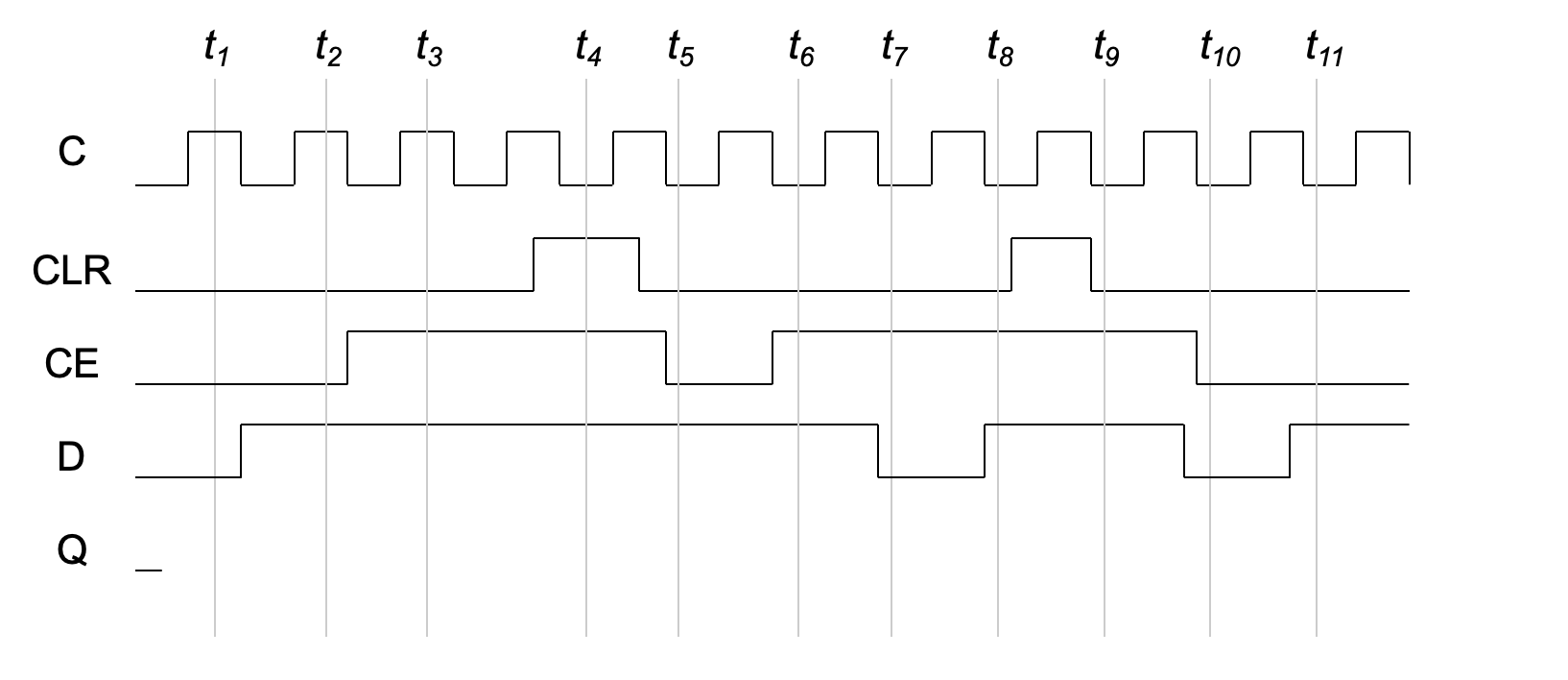
Determine the value of the output ‘Q’ of the FDCE element based on the inputs from the waveform shown below. Note that the CLR input is asynchronous, meaning it takes effect immediately when asserted, and does not wait for a clock edge.
The SystemVerilog example below demonstrates how to instance a single FDCE flip-flop into a design:
FDCE my_ff (.Q(ff_output), .C(CLK), .CE(1'b1), .CLR(1'b0), .D(ff_input));
The example shown above assigns a constant zero to the CLR input and a constant one to the clock enable (CE), essentially disabling those functions. As a result, the code above is basically a D flip-flop with input D, output Q and a clock C. NOTE: as the documentation describes, this is a rising edge triggered flip-flop.
Exercises
Make sure to merge in any changes from the startercode before starting the lab.
Exercise #1: 4-bit Register
In this exercise you will create a 4-bit register that can store 4-bit values.
This register will be used in a later exercise to create a register file.
Begin this exercise by creating a module name reg4 in a file reg4/reg4.sv with the following ports:
| Module Name: reg4 | |||
|---|---|---|---|
| Port Name | Direction | Width | Function |
| clk | Input | 1 | Clock input |
| din | Input | 4 | Data to be loaded into register |
| load | Input | 1 | Control signal to cause register to load |
| clr | Input | 1 | Control signal to clear the contents of the register |
| q | Output | 4 | Register output |
This register should be created by instancing four FDCE flip-flops (one for each register bit) as shown above in the preliminary. Each flip-flop will form one of the four bits of the register. Attach the module ports to each of the flip-flops as follows:
- Attach the
clkinput to theCinput of each flip-flop - Attach the
loadinput to theCEinput of each flip-flop - Attach the
clrinput to theCLRinput of each flip-flop - Attach a different bit of the
dinsignal to theDinputs of the four different flop-flops - Attach a different bit of the
qoutput signal to theQoutputs of the four different flip-flops After completing your register, simulate your register to demonstrate to yourself that it is working correctly.
Once you have prepared the simulation environment, you are ready to simulate your module.
Create a Tcl simulation script named sim.tcl and include it in your repository.
This script should be written to do the following:
- Create an oscillating clock input (see instructions below)
- Run the clock for at least two clock cycles without setting any input signals
- Set all non-clock input signals to zero
- Run the clock for at least 10 clock cycles with all the non-clock input signals set to zero
- Set the
dininput to a non-zero value - Set the
loadsignal to one for at least one clock cycle and then setloadback to zero for at least one clock signal (make sure thedinpropagates toq) - Demonstrate the loading of at least three other values to the register
- Clear the register by asserting the
clrsignal to demonstrate the clear functionality - Load at least one more value to the register
For this simulation you will need to simulate an oscillating clock.
Rather than provide a Tcl command for each rising and falling edge of the clock, you can add additional arguments to the add_force command to cause the signal to oscillate.
The following example demonstrates a Tcl command that will generate an oscillating clock input.
# add oscillating clock input with 10ns period
add_force clk {0 0} {1 5ns} -repeat_every 10ns
The first parameter after the signal name, {0 0}, indicates that the signal should be set to zero initially.
The first parameter after the signal name, {1 5ns}, indicates that the signal should change to one after 5 nanoseconds (half of a 100Mhz clock period).
The final parameter, -repeat_every 10ns, indicates that this sequence should continue every 10ns to simulate a continuous clock.
After creating your simulation .tcl file, simulate your register to demonstrate to yourself that it is working correctly.
When it is working correctly, take a screenshot of the simulation and save it in a file named sim.png.
Include this file in your repository.
Include the file reg4/reg4.sv in your repository.
Include the file reg4/sim.tcl in your repository.
Include the file reg4/sim.png in your repository.
Exercise #2: Register File
In this exercise you will take the 4-bit register file you created in the previous exercise and create a register file with 8 entries. This register file will allow you to save eight different 4-bit numbers based using a 3-bit address to indicate which of the eight registers you want to read from or write to.
Begin by creating a file named regfile/regfile.sv with a module named regfile with the ports as shown in the table below:
| Module Name: regfile | |||
|---|---|---|---|
| Port Name | Direction | Width | Function |
| clk | Input | 1 | Clock input |
| din | Input | 4 | Data to be loaded into register |
| addr | Input | 3 | Address to specify the register to read/load |
| load | Input | 1 | Control signal to cause register to load |
| clr | Input | 1 | Control signal to clear the contents of the register |
| q | Output | 4 | Register output |
- Instance eight copies of your
reg4module developed in the previous exercise. - Connect the
clk,din, andclrinputs to the corresponding ports of each of thereg4modules. - Create a unique 4-bit signal for the
qoutput of each of the 8 registers. - Create a multiplexer that assigns the value of the
qoutput of theregfilemodule based on the value of theaddrinput. For example, if theaddrinput is a010, theqoutput of the register file should be the value of the 2nd register file (i.e., 010 = 2). Consider using the ternary operator (? :) to build the multiplexer. - Create a decoder that decodes the
addrinput to generate eight different decode outputs. Use these decoder signals along with theloadinput signal to generate a selective load signal for each of the eight registers. For example, if theloadinput signal is high and theaddrinput is101then the load signal of the 5th register should be high (i.e., 101 = 5). Refer to Figure 19.1 from the textbook for a visual representation of the register file you are creating.
A testbench has been provided to test your register file.
Run the testbench (make sim_tb), and make sure your design is working correctly before moving on to the next exercise.
What is the time in nano seconds in which the simulation ends?
What is the value of register 3 at time 480ns?
At what time is the clr signal asserted in the simulation?
Include the file regfile/regfile.sv in your repository.
Exercise #3: Top-Level Design
Create another a SystemVerilog file named regfile_top/regfile_top.sv for the top-level module that contains your register file module.
Add the following ports to your top-level module:
| Module Name: regfile_top | |||
|---|---|---|---|
| Port Name | Direction | Width | Function |
| clk | Input | 1 | 100 MHz clock |
| data_in | Input | 4 | Data input (switches[3:0]) |
| addr | Input | 3 | Register address (switches[15:13]) |
| btnc | Input | 1 | Write register file |
| btnd | Input | 1 | Clear register file |
| btnr | Input | 1 | Right button (will turn off all digits when pressed) |
| segment | Output | 8 | Cathode segments |
| anode | Output | 4 | Anode signals for each of the four digits |
Design your top-level module as follows:
- Instance your register file module and connect the ports as described below:
- Connect the top-level
clkinput to theclkport of the register file - Connect btnc to the
loadport - Connect btnd to the
clrport - Connect data_in (
switches[3:0]) to thedinport - Connect addr (
switches[15:13]) to theaddrport
- Connect the top-level
- Instance your seven segment display module from your previous lab
- Connect the output from the register file to the
datainput of the seven segment display - Connect the
segmentsfrom the seven segment display to the top-levelsegmentports - Assign
segment[7]for the digit point such that the digit point is not displayed (i.e., don’t display the digit point) - Assign the top-level anode values such that only the right-most digit is displayed.
- Make sure
btnrturns off all digits when pressed.
- Connect the output from the register file to the
Include the file regfile_top/regfile_top.sv in your repository.
Exercise #4: Synthesize
Create a regfile_top/basys3.xdc file for your top-level design to map the top-level ports to pins on the Basys3 board.
When using a clock for designs with sequential logic, you must add a special constraint for the clock port.
The following example demonstrates how to add this constraint for the clk port:
set_property -dict { PACKAGE_PIN W5   IOSTANDARD LVCMOS33 } [get_ports clk]
create_clock -add -name sys_clk_pin -period 10.00 -waveform {0 5} [get_ports clk]
The first line assigns the clk port to pin W5 on the Basys3 board as is done with all other top-level pins.
The second line defines a clock and specifies the clock period for use by the timing analyzer.
Run synthesis, and carefully review the synthesis log to make sure there are no warnings. Answer the following questions from the synthesis log.
How many FDCE cells are used by the design?
How many total LUT resources are used by the design? (add up all the LUT* resources)
What primitive cell is used to drive the global clock? (it begins with ‘B’)
Include the file regfile_top/basys3.xdc in your repository.
Exercise #5: Implementation and Download
Run implementation, and review the implementation log to make sure there are no warnings.
Download the bitstream to make sure the design is operating as you expect (including the operation of the seven segment display).
Test the design by loading values in to the register file at different addresses and then going back to make sure the values are still correct.
Test the ability to clear the register file with the btnd.
Note that the TAs will carefully test your bitstream to make sure that it operates correctly.
Congratulations! You have designed your first sequential circuit.
Open the implemented design (review Vivado Device Viewer Section of the Common Makefile Tutorial if needed).
Find the IBUF cell that is used for the clock input buffer and take a screenshot. Name this file fpga.png
Include the file regfile_top/fpga.png in your repository.
Final Pass-Off
Refer to the passoff tutorial for the passoff process.
- See
required_filesin the passoff script. - Makefile rules that must work correctly and be free from errors and warnings:
Makefile:cleanregfile/Makefile:sim_tbregfile_top/Makefile:synth,implement
Answer the final two questions in your laboratory report:
How many hours did you work on the lab?
Provide any suggestions for improving this lab in the future