Table of Contents
Overview
In this lab you will be given a secret message that has been encrypted with a secret key. You will create a circuit that tries every possible key until you find out which key successfully decrypts the message.
Your design will start searching for the key after the center button is pressed. The current key being tried is displayed on the LEDs, and your stopwatch from a previous lab is used to time how long it takes for you to find the correct key. Once you have discovered the secret message, you will display this secret message on your own computer using a serial terminal emulator called “PuTTY”.
In the video below, the message is displayed on a VGA monitor rather than in PuTTY. But, for this term you will display the message in PuTTY.
The progression of the exercises is:
- Exercise 1: Set up your project, and draw a message of your choosing on the screen.
- Exercise 2 and 3: You will be given an encrypted message, and the decryption key. You will decrypt the message, and display the decrypted message in PuTTY.
- Exercise 4: You will be given an encrypted message, but not the decryption key. You will search through all keys to find the key that properly decrypts a given message, and then display the decoded message.
The average time to complete this lab is 4.5 hours.
Learning Outcomes
- Implement a state machine using behavioral SystemVerilog
- Build a system in SystemVerilog that contains several interacting modules.
Preliminary
ASCII Character Values
In computer systems, we typically use an 8-bit number to represent different characters, including uppercase (A, B, C, …) and lowercase (a, b, c, …) alphabet characters, digits (0, 1, 2, …), symbols ($, %, ^, …) and special characters (space, tab, new line). Online, you can easily find an ASCII Table that lists the integer values we use for each of these characters. Almost all computers and electronics you will encounter use these same standardized ASCII values. When you consult this table, be mindful that the values are typically listed in both decimal and hexadecimal, so be sure you are looking at the correct column!
- What is the hexadecimal ASCII value for character
D? - What is the hexadecimal ASCII value for character
d? - What character is represented by the ASCII value
0x09?
Encryption
This lab is all about encryption and decryption, but it may be the first time you’ve learned about these things. At the most basic level, an encryption process takes two inputs: a message (we call plaintext) and a secret key (we call the key). It produces an encrypted message, called the cyphertext. Decryption is the reverse process. It takes the cyphertext and the same original key, and produces the original plaintext.
In this lab we will be using the RC4 encryption algorithm. It’s an old encryption algorithm, and don’t worry, you don’t need to understand how it works. What’s important to know for our system is that we are going to use messages that are 16 bytes long (128 bits), and a 24 bit key.
- How many different key values can our system have?
As an example, we may have a 16 byte message, “WE LOVE ECEN 220”, which we can assign to logic in SystemVerilog like this:
logic [127:0] plaintext;
assign plaintext = {8'h57, 8'h45, 8'h20, 8'h4C, 8'h4F, 8'h56, 8'h45, 8'h20, 8'h45, 8'h43, 8'h45, 8'h4E, 8'h20, 8'h32, 8'h32, 8'h30};
// The above is split up to show the individual bytes, we could also store it like this:
assign plaintext = 128'h5745204C4F5645204543454E20323230;
// Or like this:
assign plaintext = {"W", "E", " ", "L", "O", "V", "E", " ", "E", "C", "E", "N", " ", "2", "2", "0"};
// Or like this:
assign plaintext = {"WE LOVE ECEN 220"};
// All of the above assign the plaintext to an identical value
If we encrypt this message using the following key:
logic [23:0] key;
assign key = 24'h010203;
then the resulting cyphertext will be equal to 128'h5c057e9fd5458ec36d7ef9cc4d23ea3e. If you look up these values in the ASCII table, you will see that the cyphertext is not a readable message. For example, the first byte, 5c is for character \, and some of the bytes (such as ea) aren’t even valid ASCII character values.
If we decrypt this cyphertext with the same key, we will get back the original message. If we use the wrong key, we will get another unreadable message.
(If you’re interested, you can try this out on https://cryptii.com/pipes/rc4-encryption. Just keep in mind you need to reverse the bytes of the key. If you choose key = 24'h010203;, then enter 03 02 01 for the key on the website).
In this lab you will be given the cyphertext, and then you need to try all of the keys until you find one that produces a readable message. Then you will have hacked the system and figured out the key!
You might be worried that you will find a key that produces a readable message, but it is not the correct key. Don’t worry, the odds of this are extremely unlikely (and we’ve double checked that this won’t happen with the encrypted messages we give you).
Modules
Once you’ve figured out the key and decrypted the secret message, you will want to display it. Unfortunately there’s no easy way to display messages like this on the board, so you will use a UART transmitter and PuTTY to display the secret message.
You can download the following modules and add them to your Vivado project:
- The decrypt_rc4 module. This module performs the decryption. You will provide a 128-bit message, a 24-bit key, and a start signal. It will take some time to perform the decryption, and then it will raise its
doneoutput and provide the decrypted message. - The CharDrawer_serial module. You provide this module with a 128-bit ASCII message and a
startsignal. If you look inside it, you will see that it instances a UART transmitter. - A clk_generator module that generates two clocks for this design. THIS IS A VERILOG FILE – don’t add it to your project as a SystemVerilog file or you will get errors.
- The SevenSegmentControl module. As in other labs, this will drive the 7-segment display.
From a previous lab, you will also need the following added to your project:
- The stopwatch module. You will use this module to time how long it takes to crack the code.
- The tx module. This module is needed to serialize the characters for output. It is instantiated by the CharDrawer_serial module.
Configuring PuTTY
PuTTY is a terminal emulation program installed on lab machines. Characters sent from your FPGA can be seen by running PuTTY and connecting to the USB serial device (/dev/ttyUSB1 on lab machines). Configure the serial device for 19200 baud, 8 bits, 1 stop bit, ODD parity, and NO flow control. Run PuTTY from the command line by typing putty or launch it from the application menu. From the PuTTY Configuration dialog, click on “Serial” in the “Category:” window on the left side to set the serial port options. You may need to scroll down to see it. Click “Open” to start a session.
Exercises
A significant portion of the modules needed for this lab have been provided for you or were created in a previous lab. For this lab, you only need to create the Codebreaker module. Almost everything you design will be contained in the Codebreaker module that you will implement shortly.
Exercise #1 - Draw a message on the screen
In this first exercise, your Codebreaker module will be very simple. Rather than break any codes you will just hardwire a plaintext to the CharDrawer_serial module and wire the request signal high. In response, the CharDrawer_serial module will display your message on the serial port (which you will see when you have PuTTY running).
Top-Level Module
The top-level module is Codebreaker_serial_top. Download it here: codebreaker_serial_top.sv. You shouldn’t need to modify it (except perhaps for your personal exploration).
Look over the code and carefully draw a block diagram of it to make sure you understand how it works. Be sure to include all signals. Top-level ports tie to things on the board that you should already be familiar with (LEDs, buttons, seven segments, …).
The module contains:
- A
clk_generatorinstance, that generates two clocks (only one of which is being used in this design). NOTE: this is a complex circuit which is able to synthesize multiple other clocks from a single input clock. As such, it REQUIRES at least 400ns simulation time before it will output valid clock signals to the rest of your circuit.- Before you proceed, go back and re-read the previous paragraph. What it is saying is that in your .tcl file, once you start the clock going you should simulate 400ns without doing anything else just so the clock generator can initialize itself. Only then should you start resetting or doing anything else with your circuit.
- A
CharDrawer_serialinstance. It is used to send bytes out the “tx_out” port to be displayed by the “PuTTY” program. It relies on the UART transmitter to serialize bytes for output. Near the bottom of theCharDrawer_serialmodule, you can see where it instances thetxmodule. Make sure the module name and port names match your design. - The
SevenSegmentControlandstopwatchinstances, configured like the Stopwatch lab. - The
Codebreakerinstance.
Pass-off: Once you have drawn the block diagram, meet with a TA and review it. Be sure you can explain how it all hangs together. It is very important you do this before you proceed. If you don’t understand how all the pieces work together, you will likely be lost for the rest of the lab (and may, unfortunately, spend a lot of time spinning your wheels).
Next, to implement the design, complete each of the following steps:
- Create a Vivado project (remember to run the commands to configure the error messages).
- Add the top-level module to your project.
- Create an appropriate constraints file for all of the top-level ports.
- Add all other necessary modules to your project. You will need to expand the modules in the Design Sources list and look to see what sub-modules are expected and make sure you have included all necessary modules. ERROR ALERT: clk_generator.v is a Verilog file, NOT a SystemVerilog file. If you mistakenly tell Vivado it is a SystemVerilog file you will get errors about undeclared signal types.
Now create a Codebreaker module (ports listed below). Note, you do not need to include the decrypt module for this exercise since you won’t be decrypting anything.
Do the following in your Codebreaker module:
- Drive the
key_displayoutput to a 0 and drive thestopwatch_runoutput to 1. - Connect the
draw_plaintextoutput to thestartinput (which is connected tobtnc). - Drive the
plaintext_to_drawoutput with a message of your choice. - Generate the bitstream and program the board.
- Verify that your message is displayed after you press
btncon the board. Note you will then need to reset your design before it will respond a second time to abtncpress.
| Module Name = Codebreaker | |||
|---|---|---|---|
| Port Name | Direction | Width | Description |
| clk | Input | 1 | 100 MHz Input Clock |
| reset | Input | 1 | Active-high reset |
| start | Input | 1 | Begin searching for the secret key |
| key_display | Output | 16 | Display portion of current key value being tested |
| stopwatch_run | Output | 1 | Active-high enable of stopwatch |
| draw_plaintext | Output | 1 | Raise this signal to display your message |
| done_drawing_plaintext | Input | 1 | This input goes high when the message is displayed |
| plaintext_to_draw | Output | 128 | The ASCII message to display |
Once this works, you may want to save a copy of the code and associated bitfile before proceeding (since you will now modify and overwrite them).
Exercise #2 - Decrypt and Display a Single Message (SM design)
The next step of this lab is to actually decrypt and display a message. To do this, you will have to instance the decrypt_rc4 module in your Codebreaker module. Before you start modifying your SystemVerilog, you will design the state machine that interacts with the decryption module.
This exercise is entirely done on paper. Design and draw a finite state machine that:
- Waits for the start button.
- Decrypts the cyphertext and obtains the plaintext.
- Displays the plaintext message over the serial console.
- Stays in a terminating state until reset.
Inputs to your state machine:
Codebreakerinputstart.Codebreakerinputdone_drawing_plaintext.- A new signal you create connected to the
doneoutput of thedecrypt_rc4module.
Outputs of your state machine:
- A new signal you create that you should connect to the
enableinput of thedecrypt_rc4module. draw_plaintextoutput ofCodebreaker.
Remember, the decrypt_rc4 module takes some time to perform the decryption, so you will need to wait for the done output to be high before moving on to display the message on the display.
Tips:
- You can implement this in about 4 states.
- It is good to choose meaningful state names (not S1, S2, etc.) This will help you reason about and debug your state machine.
Pass-off: Share your state machine with a TA and get feedback. This is strictly to keep you from wasting a lot of time implementing a state machine which has obvious problems.
Exercise #3 - Decrypt and Display a Message
Implement your state machine in the Codebreaker module. Test your design with the following 128-bit cyphertext and 24-bit key. You should get a readable message in your simulation. You should be simulating Codebreaker_serial_top and using your own Tcl file.
assign key = 24'h79726a;
assign cyphertext = 128'h93a931affae622e10a029bd3d4bd6ced;
In order to make the decoded message be in ASCII instead of hex, change the radix of the plaintext_to_draw signal to be ASCII (right click it in the simulation waveform window to see the radix menu).
Use simulation to debug your design when necessary. As mentioned above, a reset time of at least 400 ns is required to allow the clk_generator module to begin functioning properly and get a clk signal to your Codebreaker module. Remember to use the signals of Codebreaker_serial_top and not Codebreaker in your Tcl script (for example, use ‘btnu’ and not ‘reset’).
Include a screenshot of the simulation showing the decoded message in the lab report. Show the plaintext_to_draw signal in ASCII instead of hex.
Exercise #4 - Brute-Force Key Search
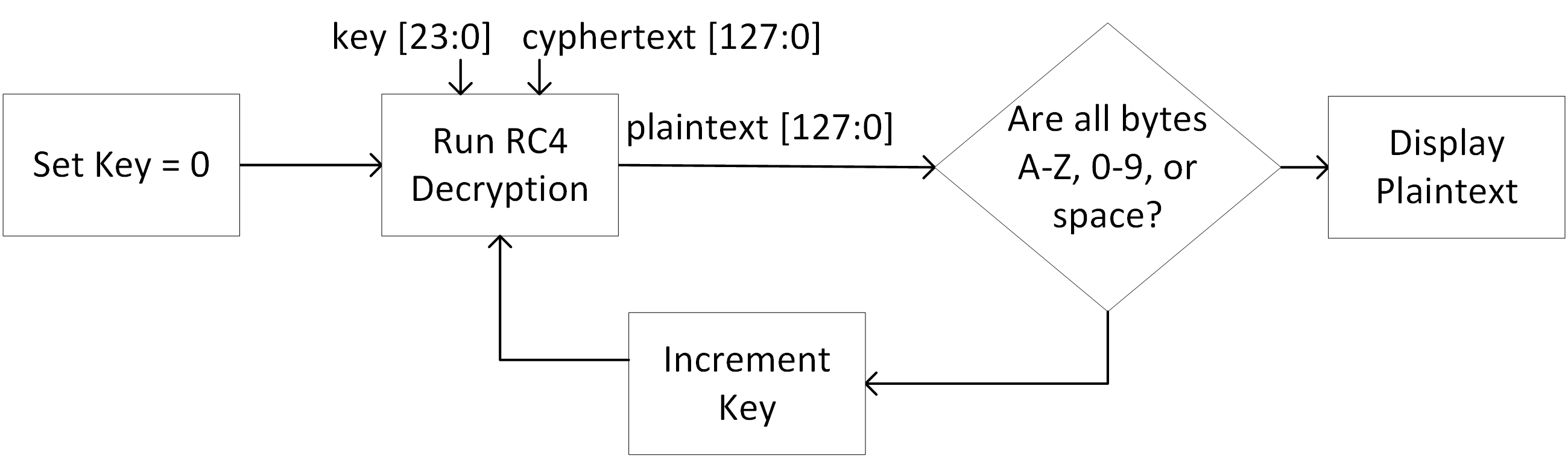
The final object of the lab is to modify your state machine to complete the above flow diagram. This consists of a system that tries every possible key value until the input cyphertext is correctly decrypted.
You know you have located the correct key when the produced plaintext only contains the characters A-Z, 0-9 or space.
Changes from the last exercise:
- You will need to add a state that checks the decrypted message and decides whether it is readable. If it is readable, you can display the message and stop, otherwise, you should continue on to the next key.
- The upper 16 bits of the key should be output on the LEDs. Although this will not show the precise key you found (since the real key is 24 bits), it will help you see that your search is progressing.
- Your state machine should have a new output that is connected to the
stopwatch_runoutput ofCodebreaker. Run the stopwatch after the user presses the button and stop once a valid plaintext message is found.
Checking that each of the 16 bytes in the plaintext is valid may require writing a very long logic expression. To save yourself some typing, we will give it to you:
// Check that each byte of the plaintext is A-Z,0-9 or space.
logic plaintext_is_ascii;
assign plaintext_is_ascii = ((plaintext_to_draw[127:120] >= "A" && plaintext_to_draw[127:120] <= "Z") || (plaintext_to_draw[127:120] >= "0" && plaintext_to_draw[127:120] <= "9") || (plaintext_to_draw[127:120] == " ")) &&
                            ((plaintext_to_draw[119:112] >= "A" && plaintext_to_draw[119:112] <= "Z") || (plaintext_to_draw[119:112] >= "0" && plaintext_to_draw[119:112] <= "9") || (plaintext_to_draw[119:112] == " ")) &&
                            ((plaintext_to_draw[111:104] >= "A" && plaintext_to_draw[111:104] <= "Z") || (plaintext_to_draw[111:104] >= "0" && plaintext_to_draw[111:104] <= "9") || (plaintext_to_draw[111:104] == " ")) &&
                            ((plaintext_to_draw[103:96] >= "A" && plaintext_to_draw[103:96] <= "Z") || (plaintext_to_draw[103:96] >= "0" && plaintext_to_draw[103:96] <= "9") || (plaintext_to_draw[103:96] == " ")) &&
                            ((plaintext_to_draw[95:88] >= "A" && plaintext_to_draw[95:88] <= "Z") || (plaintext_to_draw[95:88] >= "0" && plaintext_to_draw[95:88] <= "9") || (plaintext_to_draw[95:88] == " ")) &&
                            ((plaintext_to_draw[87:80] >= "A" && plaintext_to_draw[87:80] <= "Z") || (plaintext_to_draw[87:80] >= "0" && plaintext_to_draw[87:80] <= "9") || (plaintext_to_draw[87:80] == " ")) &&
                            ((plaintext_to_draw[79:72] >= "A" && plaintext_to_draw[79:72] <= "Z") || (plaintext_to_draw[79:72] >= "0" && plaintext_to_draw[79:72] <= "9") || (plaintext_to_draw[79:72] == " ")) &&
                            ((plaintext_to_draw[71:64] >= "A" && plaintext_to_draw[71:64] <= "Z") || (plaintext_to_draw[71:64] >= "0" && plaintext_to_draw[71:64] <= "9") || (plaintext_to_draw[71:64] == " ")) &&
                            ((plaintext_to_draw[63:56] >= "A" && plaintext_to_draw[63:56] <= "Z") || (plaintext_to_draw[63:56] >= "0" && plaintext_to_draw[63:56] <= "9") || (plaintext_to_draw[63:56] == " ")) &&
                            ((plaintext_to_draw[55:48] >= "A" && plaintext_to_draw[55:48] <= "Z") || (plaintext_to_draw[55:48] >= "0" && plaintext_to_draw[55:48] <= "9") || (plaintext_to_draw[55:48] == " ")) &&
                            ((plaintext_to_draw[47:40] >= "A" && plaintext_to_draw[47:40] <= "Z") || (plaintext_to_draw[47:40] >= "0" && plaintext_to_draw[47:40] <= "9") || (plaintext_to_draw[47:40] == " ")) &&
                            ((plaintext_to_draw[39:32] >= "A" && plaintext_to_draw[39:32] <= "Z") || (plaintext_to_draw[39:32] >= "0" && plaintext_to_draw[39:32] <= "9") || (plaintext_to_draw[39:32] == " ")) &&
                            ((plaintext_to_draw[31:24] >= "A" && plaintext_to_draw[31:24] <= "Z") || (plaintext_to_draw[31:24] >= "0" && plaintext_to_draw[31:24] <= "9") || (plaintext_to_draw[31:24] == " ")) &&
                            ((plaintext_to_draw[23:16] >= "A" && plaintext_to_draw[23:16] <= "Z") || (plaintext_to_draw[23:16] >= "0" && plaintext_to_draw[23:16] <= "9") || (plaintext_to_draw[23:16] == " ")) &&
                            ((plaintext_to_draw[15:8] >= "A" && plaintext_to_draw[15:8] <= "Z") || (plaintext_to_draw[15:8] >= "0" && plaintext_to_draw[15:8] <= "9") || (plaintext_to_draw[15:8] == " ")) &&
                            ((plaintext_to_draw[7:0] >= "A" && plaintext_to_draw[7:0] <= "Z") || (plaintext_to_draw[7:0] >= "0" && plaintext_to_draw[7:0] <= "9") || (plaintext_to_draw[7:0] == " "));
Simulate your brute-force design on the cyphertext below. HINT: the key is 000005 – be sure your circuit finds that one.
assign cyphertext = 128'hca7d05cd7e096d91acaf6fd347ef4994;
Include a screenshot of your simulation waveform demonstrating that your simulation works and finds the correct key (be sure both the key and resulting decoded text are visible in the simulation).
Exercise #5 - Synthesize and Implement
Now, synthesize and run the design you just simulated in hardware to verify that you get the right message printed to PuTTY. Note: since the key is only ‘5’ it won’t show on the LEDs because they are only displaying the top 16 bits of the 24-bit keyspace. Getting the message printed in PuTTY will be your sign that it is working.
Finally, you seem to have a working brute-force code breaker – congratulations!
Your last step is to choose one of the cyphertexts below, add it to your design, and re-synthesize/implement/bitgen and run in hardware to demonstrate that it is working. Each of these cyphertexts has a different key and will produce a different message. You are required to demonstrate your codebreaker breaking just one of them. But, you may try several to see how your design works.
assign cyphertext = 128'ha13a3ab3071897088f3233a58d6238bb;
assign cyphertext = 128'hb8935bbf5f819bcfec46da11d5393d4f;
assign cyphertext = 128'h396d6e70500754ff726bd5fb963998ce;
assign cyphertext = 128'h189f2800aac06ce4a74292bffe33fd2c;
assign cyphertext = 128'h19b39b044dc39c4e98f9dfb44a0b7c11;
Paste your synthesis logs to Learning Suite to demonstrate that you had no errors or critical warnings. If you do have any CRITICAL WARNINGS, explain the source of them and why they are OK (they likely are not OK).
A few WARNINGS do sometimes appear and they are often OK, but there is no guarantee. Carefully read them and, if in question, ask about them.
Paste your Codebreaker SystemVerilog module.
Final Pass-Off
Do the pass-off in person with a TA or by video:
Choose one of the Exercise #5 cyphertexts and demonstrate how your circuit design running on the FPGA board breaks the code. When the key is found, your system should stop with the key value showing on the LEDs and the decoded message showing on the screen. Be sure to state which cyphertext you chose (of the 5) and show precisely what key was found.
How many hours did you work on the lab?
Please provide any suggestions for improving this lab in the future.