Table of Contents
Learning Outcomes
- Learn how to implement state machines using behavioral SystemVerilog
- Understand how asynchronous communication works
- Implement an asynchronous transmitter in SystemVerilog
Preliminary
In this laboratory you will create an asynchronous serial transmitter that will allow you to send ASCII characters from the Basys3 board to your computer. Here is an introductory video:
Chapter 28 discusses the asynchronous transmitter in detail. You will want to review this chapter before beginning this lab and refer back to it when you have questions. Note that we will be using the method described in Section 28.3 (note there are at least two methods described in this section, we are doing the one reflected in Figures 28.8, 28.9, 28.11, 28.12, and programs 28.3.1).
In this lab we will operate the transmitter at a baud rate of 19,200 bits per second. We will transmit using ODD parity and 8 bits of data.
Exercises
Exercise #1 - Asynchronous Transmitter Module
Begin your laboratory assignment by creating a module named ‘tx’ in a file named tx.sv that has the following parameters and ports:
| Parameter | Default | Function |
|---|---|---|
| CLK_FREQUENCY | 100_000_000 | Specifies the frequency of the clock in Hz |
| BAUD_RATE | 19_200 | Determine the baud rate of the transmitter |
| Module Name: tx | |||
|---|---|---|---|
| Port Name | Direction | Width | Function |
| clk | Input | 1 | 100 MHz System Clock |
| rst | Input | 1 | Reset signal that is active high |
| Send | Input | 1 | Control signal to request a data transmission |
| Din | Input | 8 | 8-bit data in to send over transmitter |
| Sent | Output | 1 | Acknowledge that transmitter is done with the transmission (corresponds to the ‘ACK’ signal in Figure 28.7) |
| Sout | Output | 1 | Transmitter serial output signal |
Design the transmitter as described in Section 28.3 of the text. The control section is outlined in Figure 28.11. Each of the major pieces of the transmitter will be described below.
Baud Rate Timer
Your transmitter will need a counter that counts the number of clock cycles for a single baud period. The number of clock cycles depends on the input clock rate and the desired baud period. Create a local parameter that calculates the number of clock cycles for a single baud period based on the parameters given in the module declaration. Create a counter signal whose bit width is based on the number of clock cycles calculated (see lab 7 for a refresher on how to calculate the number of bits needed for a counter).
Create the counter using behavioral SystemVerilog with the following specifications:
- Clear the counter when the
clrTimeroutput from the state machine is asserted. - The counter should roll over to zero when it reaches the last clock cycle of the baud period.
- Create a signal
timerDonethat indicates when the counter has reached the last clock cycle of the baud period (this signal is an input to the state machine).
Bit Counter
Create the Bit Counter which is responsible for counting the number of data bits that have been transmitted (see Figure 28.11). Design the counter using behavioral SystemVerilog with the following specifications:
- Set the counter to 0 when the
clrBitoutput from the state machine is asserted. - It increments when the
incBitoutput from the state machine is asserted. - Create a signal
bitDonethat indicates when the counter has reached the last bit of the data (this signal is an input to the state machine). Note that the bit counter you use for the transmitter needs to send 8 bits rather than 7 bits as described in the textbook.
Datapath Shift Register
The next component to create is the datapath shift register. A diagram of this shift register is shown in Figure 28.10 of the textbook. This datapath approach is the “alternative” approach and different from the initial datapath described in Program 28.3.1 of the text. The purpose of this shift register is to store the contents of the bits to be sent over the serial line. It must support a parallel load when starting a transmission and must be able to shift the bits out serially one bit at a time during transmission.
Create your parallel load shift register using behavioral SystemVerilog with the following specifications:
- Create a 10-bit signal for the register (Note that you need 8 data bits instead of 7 as shown in the figure).
- This register should be set to all 1’s with a synchronous reset.
- Create a signal named
loadfor loading the register. When this signal is asserted, load each of the 10 bits of the register with the following values:- Bit 0: constant ‘0’ (start bit)
- Bits [8:1]: The 8 bits of data to be sent. The least significant data bit should be loaded into bit 1 of the register and the most significant data bit should be loaded into bit 8 of the register. Note that Figure 28.10 only uses 7 data bits, but you will need 8 data bits.
- Bit 9: parity bit (odd parity, calculated as explained in the book)
- Create a signal named
shiftfor shifting the register. When this signal is asserted, shift the bits of the register to the right by one bit (i.e., shift in a constant ‘1’ for the stop bit into the left most significant bit of the register). - The
Soutoutput signal should be assigned to the least significant bit (LSB) of the shift register. Since the shift register shifts right during transmission, the LSB contains the current bit being transmitted.
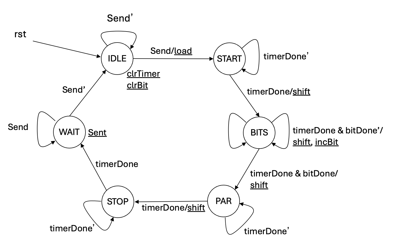
FSM
Create the FSM as outlined in the following figure. Note that this is slightly different from the one shown in the textbook.
Exercise #2 - Transmitter TCL Simulation
For this exercise you will simulate the transmitter of a single byte using a Tcl simulation script.
Create a simulation tcl script named sim_tx.tcl that performs this simulation.
This script should be written as follows:
- Start with the ‘restart’ command
- Create an oscillating clock signal with a period of 10ns
- Run the circuit for a few clock cycles without any inputs set
- Set all inputs to a default value
- Issue the reset and run for a couple of clock cycles
- Deassert the reset signal and run for a couple of clock cycles
- Set the signals to send a byte over the transmitter
- Run the simulation until the byte has finished transmitting
- Deassert the ‘Send’ signal to complete the handshaking
- Run the simulation for a few more microseconds
Look at the waveform and make sure your module is operating correctly. Verify the following points in the simulation:
- For each byte sent, Check that the 8 data bits are output correctly in the correct order.
- Check that the parity output is correct.
- Check that the start and stop output is correct.
- Check that both of your timers are operating correctly; that they reset and increment in the correct conditions.
When you are satisfied with the operation of your transmitter and the simulation output, create a screenshot of the simulation waveform and save it as sim_tx.png.
Exercise #3 - Transmitter Testbench Simulation
After simulating your module and verifying it operates with the Tcl script, you will need to test your transmitter with a testbench.
The testbench file is named tb_tx.sv and is located as part of the starter code in your lab repository.
Begin by testing the decoder interactively in GUI mode with this testbench to resolve syntax and behavioral problems in your design.
Once you have resolved these issues, create a Makefile rule named sim_tx_tb that will run the simulation of your seven-segment controller with the testbench.
This rule should generate a log file named sim_tx_tb.log.
Make sure that your testbench simulates without any errors.
What is the fourth character transmitted in the testbench?
How many characters are transmitted in the testbench?
What is the time in nano seconds in which the simulation ends?
Exercise #4 - Top-Level TX Module
Begin a new top-level module named ‘tx_top’ in a file named tx_top.sv with the following ports and parameters:
| Parameter | Default | Function |
|---|---|---|
| CLK_FREQUENCY | 100_000_000 | Specifies the frequency of the clock in Hz |
| BAUD_RATE | 19_200 | Determine the baud rate of the transmitter |
| REFRESH_RATE | 19_200 | Determine the seven segment display refresh time |
| WAIT_TIME_US | 5_000 | Determine the debouncer wait time |
| Module Name: tx_top | |||
|---|---|---|---|
| Port Name | Direction | Width | Function |
| clk | Input | 1 | 100 MHz System Clock |
| sw | Input | 8 | 8 Slide switches to specify the character to send |
| btnc | Input | 1 | Send character control signal |
| btnd | Input | 1 | Reset character control signal |
| tx_out | Output | 1 | Transmit signal |
| segment | Output | 8 | Cathode signals for the seven-segment display |
| anode | Output | 4 | Anode signals for the seven-segment display |
| tx_debug | Output | 1 | TX Debug signal |
| sent | Output | 1 | TX Sent signal |
Create the following components as part of your top-level module.
Synchronizers and Debouncer
The two input buttons need to be synchronized to the global clock. Create a two flip-flop synchronizer between ‘btnd’ and your internal reset signal. Also, create a two flip-flop synchronizer for ‘btnc’.
‘btnc’ will be used to send characters over the transmitter so it needs to be debounced to prevent multiple characters from being sent with a single button press. Instance your ‘debounce’ module and connect the synchronized ‘btnc’ signal to the ‘debounce’ module. The output of the debouncer should be connected to the ‘Send’ signal that will go into the ‘tx’ module.
Seven Segment Controller
Instance your seven-segment display controller and connect the inputs to your controller as follows:
- Attach the 8 switches to the lower 8-bits of the data in of the seven-segment controller. Assign the upper 8 bits of the data in to ‘0’.
- Only display the bottom two digits of the seven-segment display (blank out the top two digits)
- Do not use any of the digit points
- Attach the anode and segment signals of the controller to the top-level outputs of the top-level module
NOTE: To use your seven_segment4.sv module (and any other modules from previous projects you will be using here) you need to reference the module in your tcl and makefile using a relative path: ../lab07/seven_segment4.sv
and NOT by copying and pasting the module into each project.
Instance tx module
Instance your ‘tx’ module and make the following connections to your ‘tx’ module:
- Connect the top-level
clkto theclkinput of your tx module - Connect the synchronized reset signal from
btndto therstinput of your tx module - Connect the debounced
btncsignal to theSendinput of your tx module - Connect the
Soutoutput of your tx module to your top-leveltx_outoutput port - Connect the inverted value of
Soutto your top-leveltx_debugoutput port - Connect the
Sentoutput of your tx module to thesentoutput of your top-level module - Connect the
swinput to theDininput of your tx module
Once you have completed your top-level module, simulate your top-level module with a ‘tcl’ script to make sure that the buttons are properly hooked up.
Name your simulation script sim_tx_top.tcl and perform the same operations in your top-level script that you performed for your transmitter module simulation script.
You may want to copy your other tcl script and adapt the signal names for the top-level.
Note that you will need to assert btnc for a long time get the signal to pass through the debouncer.
When you have completed the simulation, create a screenshot of the simulation waveform and save it as sim_tx_top.png.
Exercise #5 - Implementation
Once you are satisfied with your top-level circuit’s behavior, create a .xdc file that contains pin location definitions for each of your I/O ports. Add .xdc entries for the clk, sw, btnc, btnd, segment, and anode top-level ports. Add the other top-level ports as follows:
tx_out: Attach the tx_out signal to the Basys3 board’s USB UART transmitter pinA18(RsTx)tx_debug: attach this signal toled[0]sent: attach this signal toled[15]
Create a Makefile rule named synth that runs the synthesis script and generates a log named synthesis.log and a ‘.dcp’ file named tx_top_synth.dcp.
Carefully review the synthesis log to make sure there are no Warnings.
How many FDxE cells are used by the design?
How many total LUT resources are used by the design? (add up all the LUT* resources)
How many total IBUF and OBUF resources do you have in the design?
After successfully synthesizing your design, begin the implementation process by creating a Makefile rule named implement that runs an implementation tcl script.
This rule should generate a log named implement.log, a ‘.dcp’ file named tx_top.dcp, a ‘.bit’ file named tx_top.bit, a utilization report named utilization.rpt, and a timing report named timing.rpt.
Review the ‘utilization.rpt’ file to answer the following questions.
How many ‘Slice LUTs’ are used by your design?
How many ‘Slice Registers’ are used by your design?
Review the ‘timing.rpt’ file to answer the following questions.
What is the Worst Negative Slack or ‘WNS’ of your design?
How many TNS total Endpoints are there in your design?
Exercise #6 - Download and Test
Once the bitstream has been generated, download your bitstream to the FPGA. To test the transmitter, you will need to run a terminal emulator program such as ‘putty’ (you used this in lab 1). Review the instructions for connecting your transmitter with PuTTY in the PuTTY tutorial. Set the baud rate to 19,200, 8 data bits, ODD parity, and 1 stop bit and connect to the appropriate COM port. Test your design and make sure you can successfully transmit characters from the Basys3 board to your computer.
Once you have a working transmitter, clear the putty screen and enter the following characters on the terminal: <netid>:<slice count> where ‘slice count’ is the total number of slices your top-level design used (e.g. mjw:100).
Review the ‘utilization.rpt’ to find the number of FPGA slices.
Take a picture of the terminal screen showing the characters you entered and save it as tx_demo.png.
Include this image in your repository.
Final Pass-Off:
- Required Files
tx.svsim_tx.tclsim_tx.pngtx_top.svsim_tx_top.tclsim_tx_top.pngtx_demo.png
- Required Makefile ‘rules’
sim_tx_tb: generatessim_tx_tb.logsynth: requirestx.sv,tx_top.sv; generatessynthesis.log,tx_top_synth.dcpimplement: requirestx_top_synth.dcp; generatesimplement.log,tx_top.dcp,tx_top.bit,utilization.rpt, andtiming.rpt
Answer the final two questions in your laboratory report:
How many hours did you work on the lab?
Provide any suggestions for improving this lab in the future