Table of Contents
The average time to complete this lab is 4.2 hours.
Learning Outcomes
You will create a debounce state machine and use this state machine to debounce the button on the Basys3 board to reliably count the number of times the button is pressed.
- Understand how to debounce noisy input signals.
- Demonstrate the ability to synchronize an asynchronous input.
- Demonstrate the benefits of a debounce circuit used to count button presses.
- Implement a state machine using behavioral SystemVerilog.
Preliminary
Carefully read and review Chapter 26 of the textbook. This lab will closely follow the design described in Chapter 26. Figure 26.1 in the textbook demonstrates the “noise” that occurs with mechanical buttons or switches. In this figure, the button signal starts at zero, transitions between zero and one, and then settles down to one. But, the same noise can happen when the button signal later transitions from one to zero.
The key principle in a denouncing circuit is to make sure the ‘noisy’ signal is stable for a predetermined amount of time before considering the signal to be valid. In the example of Figure 26.2 in the textbook, a time of 5 ms is used. The debouncer circuit in this example needs to make sure that the noisy signal is stable for 5 ms before considering the signal to be valid.
Assuming a 100 MHz clock (10 ns period), how many clock cycles are needed to implement a delay of 5 ms in the debouncing circuit?
How many bits are needed for a counter to implement a 5 ms delay with a 100 MHz clock?
The state machine for the debouncer is shown in Figure 26.4 of the textbook. Answer the following questions about this state machine.
What is the purpose of the S0 state?
What is the purpose of the S1 state?
What is the purpose of the S2 state?
What is the purpose of the S3 state?
In addition to a debouncer, your top-level circuit will need to include a “one shot” detector (see Section 26.2 of the textbook). The purpose of this circuit is to generate a single cycle pulse when a transition between low and high occurs on the debounced signal.
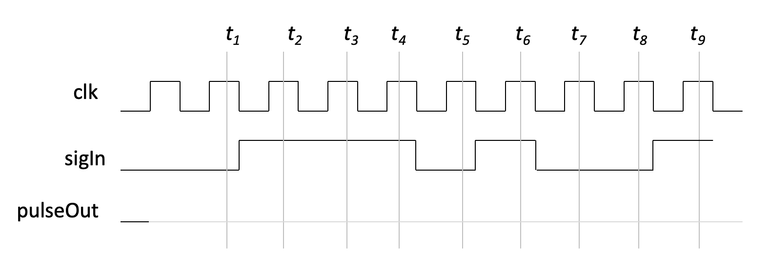
Determine the value of the pulseOut signal during each clock cycle of the following waveform.
Exercises
Exercise #1 - Debounce State Machine
Begin this exercise by creating a module named debounce in a file debounce.sv and add the ports and parameters for your module as described below:
| Parameter | Default | Function |
|---|---|---|
| WAIT_TIME_US | 5000 | Determines the wait time, in micro seconds, for the debounce circuit |
| CLK_FREQUENCY | 100_000_000 | Specifies the frequency of the clock in Hz |
| Module Name: debounce | |||
|---|---|---|---|
| Port Name | Direction | Width | Function |
| clk | Input | 1 | Clock |
| rst | Input | 1 | Active high synchronous reset |
| noisy | Input | 1 | Noisy debounce input |
| debounced | Output | 1 | Debounced output |
As shown in Figure 26.3, the debounce circuit described in Chapter 26 is composed of two parts: a timer and a state machine. You will need to create both of these parts within the module as described in detail below.
Debounce Timer
The first part of the debounce circuit is the debounce timer. The purpose of this timer is to wait a predetermined amount of time for the noise input signal to settle down before considering the signal to be valid. Like the multi-seven segment display in Lab 7, your timer must be parameterizable so that it can support an arbitrary timer wait count for the debouncer. The number of clock cycles needed for the timer depends on the module parameters ‘CLK_FREQUENCY’ and ‘WAIT_TIME_US’.
Create a localparam named ‘TIMER_CLOCK_COUNT’ that indicates the number of clock cycles used for the timer in your state machine:
localparam TIMER_CLOCK_COUNT = (CLK_FREQUENCY / 1_000_000) * WAIT_TIME_US;
Note that in this equation the frequency is divided by 1,000,000 to convert the frequency from Hz to MHz. The multiplication by ‘WAIT_TIME_US’ converts the wait time from microseconds to seconds (this multiplication occurs after the divide since multiplying before the divide may result in an integer overflow). Determine the number of bits needed to represent the ‘TIMER_CLOCK_COUNT’ value using the ‘clog2’ function and declare a local signal to represent the timer count (see Lab 7 for an example on how to do this).
After declaring your timer signal, design your timer counter as follows:
- If the ‘clrTimer’ signal is asserted, the timer should be cleared to zero.
- Otherwise, the timer should increment
- If the timer reaches the ‘TIMER_CLOCK_COUNT-1’ value, the ‘timerDone’ signal should be asserted. In addition, the timer should be cleared to zero.
Debounce State Machine
The second part of this debounce circuit is the debounce finite state machine (Figure 26.4). The inputs to the state machine are “noisy”, which is a module input and “timerDone”, which is an internal signal generated by the timer. The outputs of the state machine are the signals “debounced”, which is a module output, and an internal signal named “clrTimer” to clear the timer.
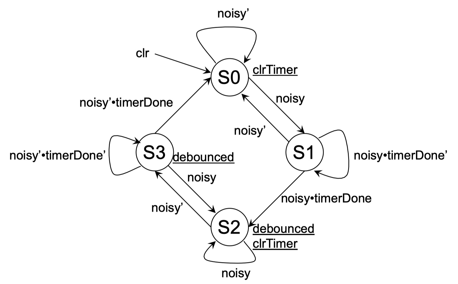
The diagram above shows a clr signal that resets/initializes your state machine.
You should use your rst input to set your state machine to S0 (synchronously).
Exercise #2 - Debounce Simulation
After completing your SystemVerilog module, you will need to simulate your module to make sure it operates as described in the textbook.
Create a Tcl simulation script named sim_debounce.tcl that simulates your debounce module with the following conditions:
- Generate a free running clock
- Issue the reset pulse
- Generate a “short” noisy positive pulse that is not long enough to generate a valid debounce output
- A “long” noisy pulse that is long enough to generate a valid debounce output
- Wait enough time to see that debounced goes low after noisy goes low
After completing your simulation, create a screenshot of your simulation waveform when zoomed out and include it in your lab report.
Name this screenshot sim_debounce.png
A testbench named tb_debounce.v has been provided in the starter code to help you simulate your debounce module.
Create a Makefile rule named sim_debounce that will run the simulation of your debouncer with the testbench.
This rule should generate a log file named sim_debounce.log.
Make sure that your testbench simulates without any errors.
Create a second Makefile rule named sim_debounce_50 that will run the testbench simulation using a parameter of WAIT_TIME_US = 50.
This rule should generate a log file named sim_debounce_50.log.
As described in earlier labs, you will need to change the parameter of WAIT_TIME_US during the elaboration step.
The following example demonstrates how this is done:
xelab --debug typical tb_debounce --generic_top "WAIT_TIME_US=50" --nolog
What is the time in nano seconds in which the first testbench simulation ends?
What is the time in nano seconds in which the second testbench simulation ends (WAIT_TIME_US=50)?
How many clock cycles of wait time are required for the WAIT_TIME_US=50 condition?
Exercise #3 - Top-Level Push Button Counter
For this exercise, you will create a top-level circuit that instances the debounce circuit for debouncing one of the push buttons. This debounce circuit will be used to increment a counter to verify that the counter increments only once for each button press. In addition to the debounce circuit, you will include a second counter that responds to undebounced button presses. You will compare the values of the two different counters to see the impact of debouncing.
Begin this exercise by creating a SystemVerilog module named debounce_top.sv with the following name and top-level ports:
| Parameter | Default | Function |
|---|---|---|
| CLK_FREQUENCY | 100_000_000 | Specifies the frequency of the clock in Hz |
| WAIT_TIME_US | 5000 | Determines the wait time, in micro seconds, for the debounce circuit |
| REFRESH_RATE | 200 | Refresh rate for seven segment controller |
| Module Name: debounce_top | |||
|---|---|---|---|
| Port Name | Direction | Width | Function |
| clk | Input | 1 | 100 MHz System Clock |
| btnd | Input | 1 | Active high reset |
| btnc | Input | 1 | Counter button input |
| anode | Output | 4 | Seven-Segment Display anode outputs |
| segment | Output | 8 | Seven-Segment Display cathode segment outputs |
The top-level module will include several components each of which are described below.
Reset Synchronizer
The reset signal should be synchronized with the global clock. Because this button signal is not synchronized to the clock, it is possible that an asynchronous reset will violate the setup/hold time constraints of the flip-flops that use the rest. You can synchronize the signal by feeding it through two flip flips, as described in Section 24.3 and shown in Figure 24.3 (the textbook uses only one flip-flop – you will need to use two). The input to these two flip-flops is ‘btnd’ and the output is the ‘reset’ signal used by the rest of the circuit.
Debounce Counter
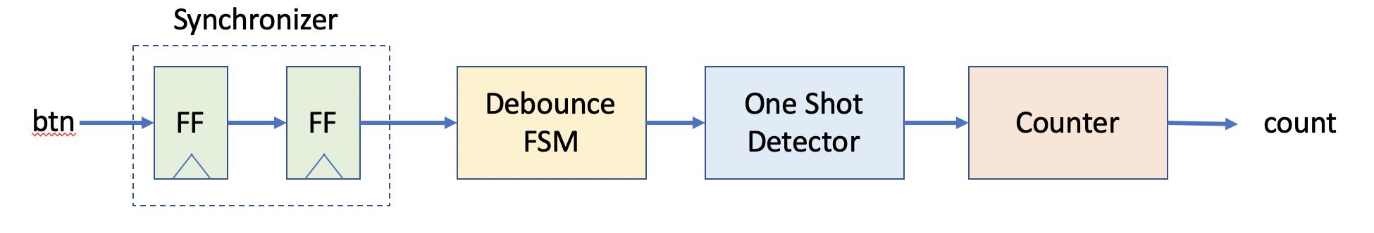
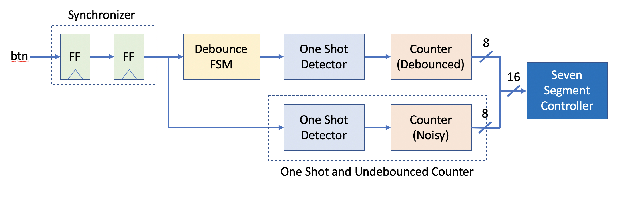
The purpose of this circuit is to accurately count the number of times a button has been pressed. Although this function sounds simple, it takes some effort to create a circuit to reliably count button presses. There are four specific components that are needed to create this circuit (see figure below):
- Synchronizer
- Debounce State Machine
- One-Shot edge detector
- Counter
-
The first part of this circuit is the “synchronizer” to synchronize the button signal to the global system clock (as described above with the reset synchronizer).
-
Instance your ‘debounce’ module and attach the output of the synchronizer to the input of your debounce module. The output of your module is now a synchronized, debounced version of the button input.
-
Add the “edge detector” circuit (also known as a ‘one shot detector’). The purpose of this circuit is to create a single clock cycle pulse when the debounced button signal transitions from a zero to a one. This single clock cycle pulse will be used to increment the button counter. If you attach the output of the debounce state machine directly into the input of your counter, the counter will increment continuously for as long as the button is pressed. The one shot is added to make sure that the counter is only incremented once each time the button goes through a 0->1 transition. A one shot circuit can be implemented by feeding a signal through two flip-flops (F1, then F2) and then outputting the equation
F1 AND F2'. This is shown in Figure 26.5 of the textbook. -
The final part of this circuit is a counter that counts the button transitions. Create an 8-bit counter with an enable input. Attach the enable signal to the output of the one shot circuit. Use the reset input to clear this counter.
Undebounced Counter
To demonstrate the behavior of the debounce circuit, a second counter is added to the top-level design which is incremented using a signal that is not debounced. The behavior of this counter will be contrasted with the debounced counter. You will use ‘btnc’ as the input, the reset signal to clear, the synchronizer, an edge detector (one shot) circuit, and an 8-bit counter, but you will not use a debouncer. You can see this additional one shot and counter in the figure below.
Seven-Segment Display
After creating your two counters, instance the multi-segment seven segment display and connect the seven-segment display as described below:
- You will use all 4 digits of the display
- Attach the 8-bit value of the debounced counter to the lower 8 bits of the display
- Attach the 8-bit value of the undebounced counter to the upper 8 bits of the display
- Turn on the digit point associated with the third digit (i.e., the digit point between digits 2 and 3)
NOTE: To use your seven_segment4.sv module (and any other modules from previous projects you will be using here) you need to reference the module in your tcl and makefile using a relative path: ../lab07/seven_segment4.sv
and NOT by copying and pasting the module into each project.
Your top-level design should look something like this (clock, reset not shown).
Simulation
After completing your top-level module, simulate the top-level with a ‘tcl’ script named sim_debounce_top.tcl.
This script should simulate at least one button press that includes at least three “noisy” transitions.
Verify that your design counts properly in these noisy button press situations.
Exercise #4 - Implementation and Download
Once you are satisfied with your top-level circuit’s behavior, create a .xdc file that contains pin location definitions for each of your I/O ports.
Create a Makefile rule named synth that runs the synthesis script and generates a log named synthesis.log and a ‘.dcp’ file named debounce_top_synth.dcp.
Carefully review the synthesis log to make sure there are no Warnings.
How many FDCE/FDRE cells are used by the design?
How many total LUT resources are used by the design? (add up all the LUT* resources)
How many total IBUF and OBUF resources do you have in the design?
After successfully synthesizing your design, begin the implementation process by creating a Makefile rule named implement that runs an implementation tcl script.
This rule should generate a log named implement.log, a ‘.dcp’ file named debounce_top.dcp, a ‘.bit’ file named debounce_top.bit, a utilization report named utilization.rpt, and a timing report named timing.rpt.
Review the ‘utilization.rpt’ file to answer the following questions.
Review the ‘timing.rpt’ file to answer the following questions.
What is the Worst Negative Slack or ‘WNS’ of your design?
How many TNS total Endpoints are there in your design?
Open your implemented design in Vivado (debounce_top.dcp) and view the design in the hardware implementation view.
Select the ‘BUFG’ cell associated with the clock signal and zoom into the device implementation that shows this buffer (this may be called something like ‘clk_IBUF_BUFG_inst’).
Make sure the routing is shown and take a screenshot of the resources used to create this counter.
Make sure you are not taking a screenshot of the entire device and are zoomed into the ‘bufg’ resource.
Name this screenshot bufg.png and include it in your repository.
Once the bitstream has been generated, download your bitstream to verify that it works correctly. After downloading your circuit, press the button several times to see if you can see a difference between the counter using the debounce state machine and the counter that does not use the debounce state machine. What you see will depend on just how “bouncy” your button is. It may bounce almost every time you push it or it may rarely bounce. Reset the counter and press the button 20 times.
What is the value of the undebounced counter after pressing the button 20 times?
Final Pass-Off:
- Required Files
debounce.svsim_debounce.tclsim_debounce.pngdebounce_top.svsim_debounce_top.tclbufg.png
- Required Makefile ‘rules’
sim_debounce: generatessim_debounce.logsim_debounce_50: generatessim_debounce_50.logsynth: requires../lab07/seven_segment4.sv,debounce.sv,debounce_top.sv; generatessynthesis.log,debounce_top_synth.dcpimplement: requiresdebounce_top_synth.dcp; generatesimplement.log,debounce_top.dcp,debounce_top.bit,utilization.rpt, andtiming.rpt
Answer the final two questions in your laboratory report:
How many hours did you work on the lab?
Provide any suggestions for improving this lab in the future