Table of Contents
The purpose of this laboratory is to design a circuit for generating the VGA synchronization signals. You will use this controller to create a “color bar” on the display. You will also use this controller in future labs to display other things on a VGA compatible display.
The average time to complete this lab is 5.1 hours.
Learning Outcomes
- Understand the timing signals required to drive a VGA display
- Understand how to create colors on the VGA display
- Create a reusable digital circuit for controlling the timing of a VGA display
Preliminary
In order to design a VGA controller, it is necessary to understand how the VGA display works and the timing of the synchronization signals required to drive the VGA display. This preliminary section of the lab will guide you through this information to prepare you for designing the VGA controller. Begin by reviewing the “VGA Port” section of the Basys3 Reference Manual to learn more about how the VGA is wired on the Basys3 board.
There are a number of figures and diagrams in this section that are helpful. In particular, look for the table in the manual that shows the exact pixel counts for the front porch, sync pulse, back porch, and visible area. For 640×480 at 60 Hz (with a 25 MHz pixel clock), you will see the following breakdown:
- Horizontal: 640 (display) + 16 (front porch) + 96 (sync pulse) + 48 (back porch) = 800
- Vertical: 480 (display) + 10 (front porch) + 2 (sync pulse) + 29 (back porch) = 521
These values tell you exactly when h_sync and v_sync must go low (their active phase). Although many references online show various VGA timings, you must use the Basys3’s official table for 640×480 at 60 Hz. Slight mismatches can cause display instability or no image at all.
After reviewing this section, answer the following questions in the lab report.
What pin number on the VGA connector is the HS signal connected to?
How many different color levels can be created for each of the three color VGA signals?
What is the range in voltage of the color signal (fully off to fully on)?
The voltage of each color signal is determined by a voltage divider between the 75 ohm termination resistance of the VGA display and the resistor divider circuit connected to the FPGA. What is the voltage on the RED VGA color signal when RED0=0, RED1=0, RED2=1, and RED3=1?
What values on the RED0, RED1, RED2, RED3, GRN0, GRN1, GRN2, GRN3, BLU0, BLU1, BLU2, and BLU3 signals are needed to generate the “full intensity” red color (i.e., provide the maximum analog voltage on the RED signal and the minimum analog voltage on the GREEN and BLUE signals)?
What does CRT stand for?
The VGA display requires two synchronization signals, Horizontal Sync (HS) and Vertical Sync (VS), to drive the display. The timing of these signals is critical to the proper operation of the VGA display. Carefully review the timing of the VGA signals in the VGA Port section of the Basys3 Reference Manual and answer the following questions:
What is the frequency of the pixel clock for the 640x480 VGA resolution?
What is the period of the horizontal sync signal (HS) for the 640x480 resolution?
What is the period of the vertical sync signal (VS) for the 640x480 resolution?
During the scan of one horizontal row, 640 pixels are displayed. However, additional time is needed during the horizontal scan for retracing. How many pixel clocks are needed during each horizontal sync for this retracing (i.e. how many pixel clocks are used when no pixel is displayed in a horizontal scan)?
How many frames per second are generated with this timing?
How many lines are NOT displayed during a full frame (i.e. lines that are blanked during a vertical retrace)?
How many pixel clocks is the horizontal sync signal low during a horizontal sync pulse?
How many pixel clocks is the vertical sync signal low during a vertical sync pulse?
Assuming the ‘display’ phase occurs first, determine the ordering of the four phases of a sync signal.
Do NOT proceed to the design until you have answered the questions above. If you are not able to answer these questions it will be difficult for you to complete the timing controller.
Exercises
Exercise 1 - VGA Timing Controller
Create a new file named vga_timing.sv that contains the timing generator for your VGA controller.
Create a module with the following input ports, and output ports:
| Port Name | Direction | Width | Function |
|---|---|---|---|
| clk | Input | 1 | 100 MHz Clock signal |
| rst | Input | 1 | Synchronous reset |
| h_sync | Output | 1 | Low asserted horizontal sync VGA signal |
| v_sync | Output | 1 | Low asserted vertical sync VGA signal |
| pixel_x | Output | 10 | Column of the current VGA pixel |
| pixel_y | Output | 10 | Row of the current VGA pixel |
| last_column | Output | 1 | The current pixel_x correspond to the last visible column |
| last_row | Output | 1 | The current pixel_y corresponds to the last visible row |
| blank | Output | 1 | The current pixel is part of a horizontal or vertical retrace and that the output color must be blanked. |
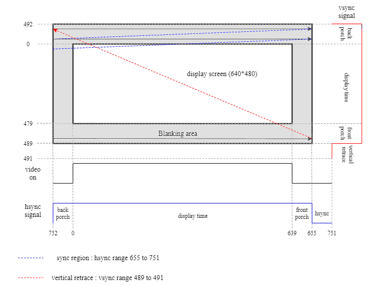
After you have created your module ports, create your VGA timing controller as described below. Also, use the following figure as reference for how these signals correspond with their respective locations on the screen. Note: Coding standard rule S19 requires that only one signal can be assigned in a ‘always_ff’ block. You will be creating multiple registers in the discussion below and need to make sure that each register is in a separate ‘always_ff’ block.
Notice that the values wrap (i.e. 0 does not start at the very end or beginning, but rather at the start of the display region):
Clock Divider Counter
For the 640x480 VGA resolution that we are implementing, the pixels change at a frequency of 25 MHz (this is called the “pixel clock”). This is four times the frequency of the 100 MHz clock that is provided with the Basys3 board. You will need to create a signal that is asserted every fourth clock cycle of the 100 MHz clock to be used by the VGA timing circuitry.
Create a signal named “pixel_en” that can be used by internal synchronous circuitry to “enable” the updating of VGA timing counters. With a 100 MHz input clock, this ‘pixel_en’ signal should be asserted every fourth clock cycle. You can generate this signal by creating a two-bit counter that sequences between the values ‘00’, ‘01’, ‘10’, and ‘11’. This synchronous counter should be set to zero when the ‘rst’ signal is asserted using a ‘synchronous’ reset. The ‘pixel_en’ signal is a combinational signal that is asserted when the counter is ‘11’.
Horizontal Pixel Counter
Create a horizontal pixel “column” counter. This counter is used to sequence through the various phases of the horizontal synch pulse (i.e., display, front porch, pulse, back porch, etc.). This counter should reset to zero when ‘rst’ is asserted (synchronous reset). Also, this counter should only update when the ‘pixel_en’ signal is asserted as described above. This counter should be designed to count through the full sequence of pixel columns including the ‘retrace’ pixel columns. For the 640x480, this counter should count from 0 to 799 (i.e. 640 displayed pixels, 16 front porch pixels, 48 back porch pixels, and 96 “pulse” pixels). When this counter is 0, it indicates that the first visible pixel is being displayed. When the counter value is 639, the counter is indicating that the last visible pixel is being displayed. When the counter is greater than 639, it indicates a column associated with the retrace phase. The output of the counter should be used to drive the ‘pixel_x’ output of your module.
Generate the “last_column” combinational output signal. This signal should be asserted when the last visible pixel in a row is being displayed (i.e. when the current column is 639).
Vertical Pixel Counter
Create a vertical pixel “row” counter.
This counter is used to sequence through the vertical sync phases and indicate the current line being displayed.
This counter should reset to zero when ‘rst’ is asserted (synchronous reset).
This counter should only update when the pixel_en signal is asserted and the horizontal counter has reached its maximum value.
When this counter is 0, it should indicate that the first visible line is being displayed.
When the counter value is 479, the counter should indicate that the last visible line is being displayed.
The output of this counter should be used to drive the ‘pixel_y’ outputs of your module.
Generate the “last_row” output signal. This combinational signal should be asserted when the last visible row is being displayed (i.e. during row 479).
Timing Signals
Your timing module needs to generate the horizontal and vertical sync timing signals (HS and VS) for the VGA display.
Remember that for VGA on the Basys3 board, h_sync and v_sync are active low. This means the signal is driven low (0) during the sync pulse, and remains high (1) at other times.
The VGA display will use these signals to synchronize the display to the VGA monitor and display the correct image on the screen.
You will generate these signals based on the values of the horizontal and vertical counters that you created above.
As described in the Basys3 Reference Manual, each timing signal has four phases:
- Display Phase (signal=1): during this phase the image is displayed on the screen.
- Front Porch Phase (signal=1): during this phase the electron beam is moved back to the left side of the screen.
- Pulse Phase (signal=0): during this phase the electron beam is moved down to the next row.
- Back Porch Phase (signal=1): during this phase the electron beam is moved back to the top of the screen.
You will use the horizontal pixel counter to determine the HS timing signal and the vertical counter to determine the VS timing signal. The following figure demonstrates the relationship between your counter and the phase of the HS timing signal:
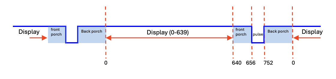
The table below summarizes each phase and the corresponding horizontal counter values for the HS signal:
| Phase | Horizontal Counter | Pixel Clocks | HS Signal |
|---|---|---|---|
| Display | 0-639 | 640 | 1 |
| Front Porch | 640-655 | 16 | 1 |
| Pulse | 656-751 | 96 | 0 |
| Back Porch | 752-799 | 48 | 1 |
Create the logic for the HS signal based on the horizontal counter as described above.
Follow the same approach as described above for the VS signal, but use the appropriate front porch, pulse, display, and back porch values for the vertical timing signal.
Here is a summary table for vertical sync timing (matching standard 640×480 @ 60 Hz from the Basys3 manual):
| Phase | Vertical Counter | Lines | VS Signal |
|---|---|---|---|
| Display | 0-479 | 480 | 1 |
| Front Porch | 480-489 | 10 | 1 |
| Pulse | 490-491 | 2 | 0 |
| Back Porch | 492-520 | 29 | 1 |
Be sure to assign v_sync = 0 only during the pulse range.
The colors on the VGA display must be set to “black” (all zero) when the timing signals are not in a display region. Using the current value of the horizontal and vertical counters, generate the ‘blank’ output signal to indicate when either the vertical or horizontal counters are not in a display region. The ‘blank’ signal will be used by higher-level modules to indicate that black must be send on the RGB color signals.
In summary:
- Horizontal counter (
pixel_x) runs 0–799:- 0–639 = visible (display)
- 640–655 = front porch
- 656–751 = sync pulse (h_sync=0)
- 752–799 = back porch
- Then it resets to 0.
- Vertical counter (
pixel_y) runs 0–520:- 0–479 = visible (display)
- 480–489 = front porch
- 490–491 = sync pulse (v_sync=0)
- 492–520 = back porch
- Then it resets to 0.
This ensures you match exactly the standard VGA timing on the Basys3. If you use these parameters and your ‘pixel_en’ runs at 25 MHz, you will achieve a 60 Hz refresh rate.
Exercise 2 - VGA Timing Controller Testbench
Like the previous labs, a testbench has been provided for you to test your VGA timing controller.
This testbench, named tb_vga_timing.sv and included in the startercode, will simulate your VGA timing controller and measure your signals to see if they follow the appropriate timing.
This testbench is very picky about timing and will complain if there are any timing problems.
Perform an initial simulation of the testbench with your vga timing controller to verify that your VGA timing controller is working correctly. Begin by simulating for only a few microseconds. If you have problems with your horizontal timing, you will see messages in a short amount of time. After resolving any of your horizontal timing problems, simulate for a longer period of time to see if your vertical timing is correct. Continue simulating and debugging until you do not see any error messages from the testbench. You will need to simulate for a relatively long period of time until the “simulation done” message appears.
Once you have resolved any issues with running the testbench manually, create a Makefile rule named sim_vga_timing that will run the simulation of your seven-segment controller with the testbench.
This rule should generate a log file named sim_vga_timing.log.
Make sure that your testbench simulates without any errors before proceeding to the next exercise.
What time in nano seconds does the blank signal go high for the vertical sync at the end of the first frame?
What time in nano seconds is the reset asserted towards the end of the simulation?
What is the time in nano seconds in which the simulation ends?
Exercise #3 - Top-level Design
Create a new file named vga_top.sv that contains the logic for generating the pixel colors on the VGA display.
Define a module named ‘vga_top’ and provide the following top-level ports:
| Port Name | Direction | Width | Function |
|---|---|---|---|
| clk | Input | 1 | 100 MHz Clock signal |
| btnd | Input | 1 | Asynchronous reset |
| btnc | Input | 1 | Display color from switches |
| btnl | Input | 1 | Display White |
| btnr | Input | 1 | Display Black |
| sw | Input | 12 | Switches to determine color to display |
| Hsync | Output | 1 | Horizontal synchronization signal |
| Vsync | Output | 1 | Vertical synchronization signal |
| vgaRed | Output | 4 | Red color signal |
| vgaGreen | Output | 4 | Green color signal |
| vgaBlue | Output | 4 | Blue color signal |
Begin your top-level design by instancing your VGA timing controller. Attach the clock and reset signals to the appropriate ports on the VGA timing controller. You can leave the signals last_column and last_row unconnected.
The primary function of your top-level design is to generate the pixel colors for the VGA display (this timing controller generated in the previous exercise does not generate the pixel color signals (RED[3:0], GREEN[3:0], and BLUE[3:0])). You will create additional circuitry that works in conjunction with your VGA timing controller to specify the color of each pixel on the VGA display.
The logic that generates the individual pixel color values will use the pixel_x and pixel_y counters within the VGA timing module to determine what color to display at the given x,y location of the VGA display. Interesting objects, images, animation, and user interfaces can be displayed by creating custom logic based on the x,y location of the VGA display. As a simple example, an image that is red on the left half of the display and green on the right half of the display can easily be created by assigning the pixel color based on the value of the pixel_x counter. The SystemVerilog code that would generate such an image is shown below (notice we always force the color to 4’b0000 in the “unused” channel):
assign red_disp   = (pixel_x < 320)  ? 4'b1111 : 4'b0000;
assign green_disp = (pixel_x >= 320) ? 4'b1111 : 4'b0000;
assign blue_disp  = 4'b0000;
In this example, when the ‘pixel_x’ counter is less than 320 (i.e., the left half of the screen), the pixel color will be red (Red=”1111”, Green=”0000”, and Blue=”0000”). When the pixel_x counter is 320 or greater, the pixel color will be green (Red=”0000”, Green=”1111”, and Blue=”0000”). More interesting and complicated images can be created with more sophisticated logic. You will create different VGA displays in future laboratory exercises.
No matter what is shown in the visible region of the VGA, the VGA pixel logic MUST send the color Black (Red=”0000”, Green=”0000”, and Blue=”0000”) during the blanking regions. A multiplexer is often used force the Black color during blanking. The following SystemVerilog code works in conjunction with the example shown above to force the color Black during blanking:
assign red   = blank ? 4'b0000 : red_disp;
assign green = blank ? 4'b0000 : green_disp;
assign blue  = blank ? 4'b0000 : blue_disp;
For this exercise, you will create the logic to generate several color patterns based on the value of the switches in priority order:
- When ‘btnd’ is pressed, assert the reset signal in your circuit. This should be tied to the rst input of the VGA timing controller. When reset, the timing controller should not generate any VGA timing signals and the VGA monitor will temporarily lose synchronization with your circuit.
- When button ‘btnr’ is pressed, display the color “Black” on the display (i.e., a blank display).
- When button ‘btnl’ is pressed, display the color White on the display.
- When button ‘btnc’ is pressed, display a single uniform color on the screen where the color is determined by the twelve switches (Red=SW[11:8], Green=SW[7:4], and Blue=SW[3:0]).
- When no buttons are pressed, create the vertical “color bar” described in the previous design exercise (see description below).
Color bars were often used in analog televisions to test the television, color, and brightness and the television transmission. The color bar you will create in this lab includes the following eight colors:
- Black: RGB=0,0,0
- Blue: RGB=0,0,f
- Green: RGB=0,f,0
- Cyan: RGB=0,f,f
- Red: RGB=f,0,0
- Magenta: RGB=f,0,f
- Yellow: RGB=f,f,0
- White: RGB=f,f,f
The vertical color bar is created by evaluating the pixel_x value to determine which of the eight colors to display. With 8 colors, each color bar should be 640 / 8 = 80 pixels wide.
You will also need a multiplexer that chooses which color pattern to display on the screen. The following example demonstrates how you could do this with a data flow statement.
assign color_out = (btnr) ? 12'h000  : // black
                   (btnl) ?          : // white
                   (btnc) ?          : // color from switches
                   vertical_color_bar; // default vertical color bar
The VGA timing signals (HS and VS) and the pixel color signals will likely contain temporary, short-term “glitches”. It is important that these glitches are not transmitted to the VGA display. Glitches on the VGA timing signals may lead to improper VGA synchronization. Glitches on the VGA colors may generate improper colors on the display. To remove the glitches, create a register for each VGA signal.
The output of the register should be wired to the corresponding FPGA output pin. The figure below demonstrates how these registers should be added:

Once you have created your top-level design, create a tcl simulation script named sim_vga_top.tcl to simulate the behavior of your top-level design.
Include this tcl script in your repository.
Your tcl simulation script should do the following:
- Create a free running clock
- Set default values for all the inputs (all buttons off, switches to 0)
- Issue the reset for a few clock cycles
- Run the simulation for ~10 vertial lines (4x800x10 clocks) so you can make sure the colors are correct. Make sure that the colors are ‘black’ during the blanking period.
- Set ‘btnl’ to high and simulate for ~10 lines to make sure the colors are white
- Set ‘btnr’ to high (and ‘btnl’ to low) and simulate for ~10 lines to make sure the colors are black
- Set ‘btnc’ to high (and ‘btnr’ and ‘btnl’ to low) and simulate for ~10 lines to make sure the colors are the same as the switches
- Run this for at least 2 different switch settings.
After simulating your top-level design, take a screenshot of the full testbench simulation waveforms and save it in a file named sim_vga_top.png.
Include this file in your repository.
Exercise 4 – Synthesis, Implementation, and Download
Once you are satisfied with your top-level circuit’s behavior, create a .xdc file that contains pin location definitions for each of your I/O ports.
Create a Makefile rule named synth that runs the synthesis script and generates a log named synthesis.log and a ‘.dcp’ file named vga_top_synth.dcp.
Carefully review the synthesis log to make sure there are no Warnings.
How many total flip-flops (FDCE or FDRE) cells are used by the design?
How many total LUT resources are used by the design? (add up all the LUT* resources)
How many total IBUF and OBUF resources do you have in the design?
After successfully synthesizing your design, begin the implementation process by creating a Makefile rule named implement that runs an implementation tcl script.
This rule should generate a log named implement.log, a ‘.dcp’ file named vga_top.dcp, a ‘.bit’ file named vga_top.bit, a utilization report named utilization.rpt, and a timing report named timing.rpt.
Instructions for generating the timing.rpt file are described in the previous lab.
After successfully implementing your design, download the bitstream to the Basys3 board and verify that the VGA controller is functioning as expected.
Review the ‘utilization.rpt’ file to answer the following questions.
How many ‘Slice LUTs’ are used by your design?
How many ‘Slice Registers’ are used by your design?
Review the ‘timing.rpt’ file to answer the following questions.
What is the Worst Negative Slack or ‘WNS’ of your design?
How many TNS total Endpoints are there in your design?
Open your implemented design in Vivado (vga_top.dcp) and view the design in the hardware implementation view.
Select the flip-flops associated with the pixel_x counter and zoom into the device implementation that shows these flip-flops.
Make sure the routing is shown and take a screenshot of the resources used to create this counter.
Make sure you are not taking a screenshot of the entire device and are zoomed into the ‘pixel_x’ counter rources.
Name this screenshot pixel_x.png and include it in your repository.
Final Pass-Off:
- Required Files
vga_timing.svvga_top.svsim_vga_top.tclsim_vga_top.pngpixel_x.png
- Required Makefile ‘rules’
sim_vga_timing: generatessim_vga_timing.logsynth: requiresvga_timing.sv,vga_top.sv; generatessynthesis.log,vga_top_synth.dcpimplement: requiresvga_top_synth.dcp; generatesimplement.log,vga_top.dcp,vga_top.bit,utilization.rpt, andtiming.rpt
Answer the final two questions in your laboratory report:
How many hours did you work on the lab?
Provide any suggestions for improving this lab in the future