Table of Contents
In this lab you will create a four-digit seven segment display controller. You will use this controller in a design that displays a 32-bit number.
The average time to complete this lab is 3.8 hours.
Learning Outcomes
- Learn how to design a sequential circuit to control a multi-digit seven segment display
- Learn how to use module parameters to specialize a module
- Learn how to read and understand timing reports
Preliminary
In Lab 5 you learned how to create a seven segment display decoder to display a single digit on the 4-digit seven segment display on the Basys3 board. For this lab, you will learn how to drive multiple digits on the display with different values. In order to do this, you will need to create a sequential counter that will control the display of each individual digit. The preliminary section of this lab will guide you through the approach for creating a multi-digit display controller.
Time Multiplexing of Digits
As described in Lab 5, all four digits share the same cathode connections to the FPGA. With this configuration, all digits will display the same value if their corresponding anode signals are asserted. You saw this in Lab 5 when the left button was pressed and all anode signals were asserted. In this case, all four digits displayed the same value as specified by the switches.
Driving the same value on all four digits isn’t that useful. Instead, we want the ability to drive each digit with a unique value so we can display a four-digit number (i.e., 16 bit hexadecimal value). To display a different value on each of the digits, you must design a controller circuit that only turns on one digit at a time and drives that digit with the appropriate segment signals. For example, to display the value “71” on the first two digits, you would assert anode signal for the first digit and drive the cathodes to display “1”. During this first period, only the first digit is being displayed. After a short period of time, the first digit is turned off and the second digit is turned on and the cathodes are driven to display “7”. This process repeats continuously in a technique called ‘time multiplexing’.
It may seem that such a technique will result in a ‘flicker’ on the display since only one digit is being displayed at any one time. However, if the rate at which each digit is turned on is fast enough, the eye cannot perceive this flicker and the display appears to be continuously illuminated. Each digit is illuminated just one-fourth of the time, but because the eye cannot perceive the darkening of a digit before it is illuminated again, the digit appears continuously illuminated. If the update, or “refresh”, rate is slowed to around 45 hertz, a flicker can be noticed in the display. For each of the four digits to appear bright and continuously illuminated, all four digits should be driven once every 1 to 16ms, for a refresh frequency of about 1KHz to 60Hz. For example, in a 62.5Hz refresh scheme, the entire display would be refreshed once every 16ms, and each digit would be illuminated for 1/4 of the refresh cycle, or 4ms. The diagram below demonstrates this refresh process.
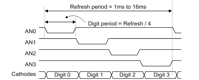
As seen in this figure, only one anode signal is asserted at a time. While one of the anode signals is asserted, the cathode signals that correspond to the digit to be displayed are also asserted. After some fixed time period, a different anode signal is asserted and the cathode signals are changed to reflect the value that should be displayed on the corresponding digit. Answer the questions below to demonstrate your understanding of the multi-segment display controller. For these questions, use the Basys3 clock frequency of 100 MHz.
Assume that your seven segment display uses a refresh rate of 1 kHz. How many clock cycles are needed for one full refresh cycle of all four digits?
How many clock cycles are needed to display a single digit using this 1 KHz example?
How many clock cycles are needed to display a single digit if the refresh rate is reduced to 250 Hz?
What will happen if the refresh is too slow?
Parameters
The seven segment display controller you are designing should be flexible to operate at a variety of refresh rates and input clock frequencies. To make your module more flexible and reusable, you will need to create parameters that can be changed when instancing your module in a design. Your module will need to include the following two parameters:
- ‘CLK_FREQUENCY’: This parameter will specify the clock frequency in Hertz of the clock input to the module. The default value is 100 MHz (100_000_000) which is the input clock rate of the Basys3 board. Providing this parameter will allow this module to be used on other boards that use a different clock rate.
- ‘REFRESH_RATE’: This parameter will specify the rate at which the 4 digit display is refreshed. The default value is 200 Hz. This parameter will allow you to change the refresh rate to suit the application needs.
Your module will use these parameters to determine how many clock cycles to display each digit. You will need to create an internal parameter to calculate the number of clock cycles to display each digit. The following example demonstrates how to create an internal parameter that performs this calculation based on the parameter values:
// Determine the number of clock cycles to display each digit
localparam DIGIT_DISPLAY_CLOCKS = CLK_FREQUENCY / REFRESH_RATE / 4;
How many clock cycles are needed to display each digit using the default parameter values?
You will need to create a counter that counts to this maximum value to control the display of each digit.
To create this counter, you will need to know the number of bits needed to represent the maximum count value.
You can use the SystemVerilog $clog2 function to make this determination.
This function computes the “ceiling” of the log base 2 of the maximum count value.
The following code segment demonstrates how to determine the number of bits to represent this maximum count and how to use this count to declare a counter signal:
// Determine the number of bits needed to represent the maximum count value
localparam DIGIT_COUNTER_WIDTH = $clog2(DIGIT_DISPLAY_CLOCKS);
// Declare a signal used for this counter signal
logic [DIGIT_COUNTER_WIDTH-1:0] digit_display_counter;
How many bits are needed to represent this maximum count value using the default parameter values?
Exercises
Exercise #1 - Multi-Digit Seven Segment Display Controller
In this first exercise, you will create a multi-segment display controller that will drive the four-digit seven segment display on the Basys3 board.
Begin by creating a file named seven_segment4.sv with the following parameters and ports:
| Module Name: seven_segment4 | ||
|---|---|---|
| Parameter | Default | Function |
| CLK_FREQUENCY | 100_000_000 | Specifies the frequency of the input clock |
| REFRESH_RATE | 200 | Specifies the display refresh rate in Hz |
| Port Name | Direction | Width | Function |
|---|---|---|---|
| clk | Input | 1 | Clock input |
| rst | Input | 1 | Reset input |
| data_in | Input | 16 | Indicates the 16-bit value to display on the 4 digits |
| blank | Input | 4 | Indicates which digits to blank |
| dp_in | Input | 4 | Indicates which digit points to display |
| segment | Output | 8 | Cathode signals for seven-segment display (including digit point). segment[0] corresponds to CA and segment[6] corresponds to CG, and segment[7] corresponds to DP. |
| anode | Output | 4 | Anode signals for each of the four digits. |
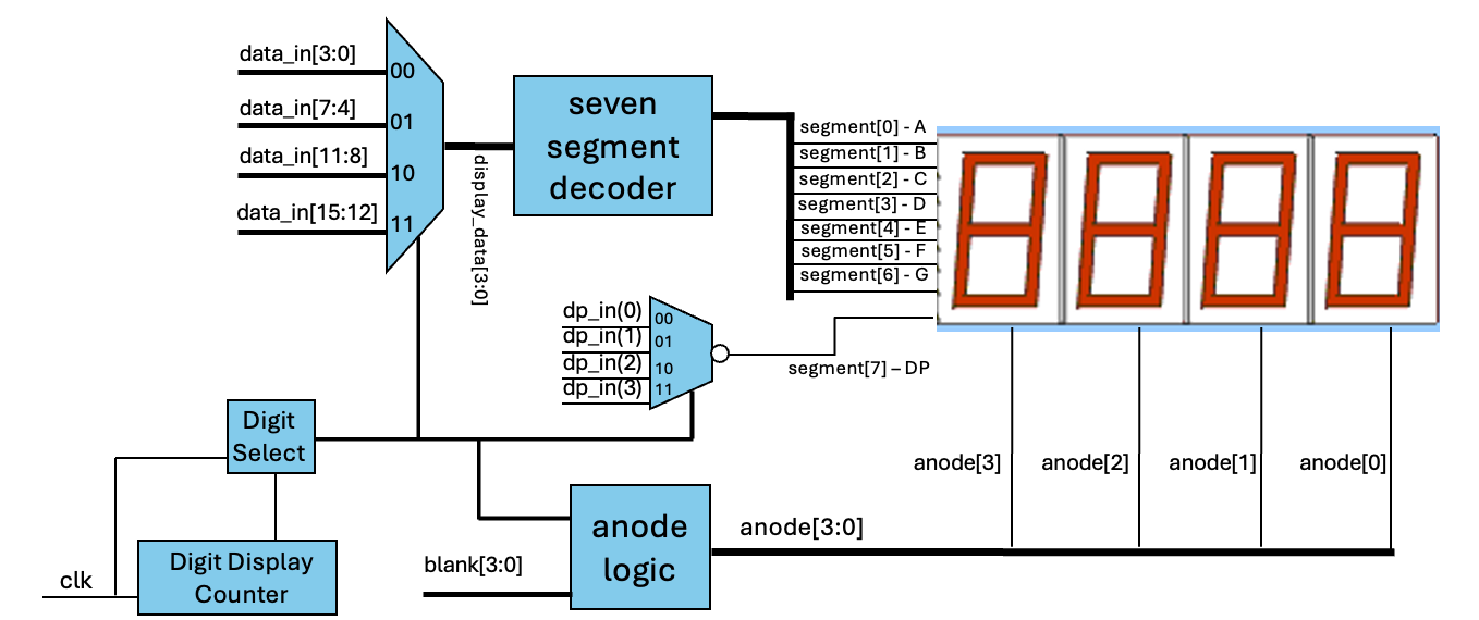
Once you have created your module definition, follow the steps outlined below to complete the module. The structure of your seven segment decoder is shown below and will be referenced in the instructions.
Step 1. Create the digit display counter
Begin your module by creating the local parameters and declaring the digit display counter signal as described in the preliminary section. Next, create a ‘free running’ counter using an ‘always_ff’ block that counts the proper number of clock cycles for displaying a digit (this is the ‘digit display counter’ referenced in the figure above). This counter should have a reset as described in class.
Next, create a two-bit counter that indicates which of the four digits to display (i.e., the ‘digit select’ counter in the figure above). This counter should increment every time the digit display counter reaches its maximum value. Like the digit display counter, this counter should be reset using a reset.
Step 2. Data In Multiplexer
Create a multiplexer that selects the appropriate 4-bit value to display based on the digit select counter. For example, if the digit select counter is ‘00’, then the first 4-bits of the data_in signal should be selected. The output of this multiplexer will be used as the input to the seven segment decoder (labeled ‘display_data’ in the figure).
Step 3. Create the seven segment decoder
Like in Lab 5, you will need to create a seven segment decoder that will convert the 4-bit binary value to display into the corresponding cathode signals for the seven segment display.
For this lab, create a new decoder using a always_comb block and a case statement.
This case statement should evaluate the ‘display_data’ signal block to select the values for segment[6:0].
You will find that this is a much simpler way of creating a decoder than was done in Lab 5.
Step 4. Create the digit point multiplexer
The dp_in[3:0] signal indicates which of the four digits should have its decimal point illuminated. Each bit corresponds to a digit point on each of the four digits. You will need to create a multiplexer that will select the appropriate value for the DP segment based on the digit select counter. Note that the digit point signal is low asserted so you will need to invert (i.e., NOT) the value selected by the multiplexer.
Step 5. Create the anode logic
Create combinational logic for the anode signals. The logic is based on the digit select counter (i.e., assign one bit of the anode signal to 0 when the appropriate digit is selected). This logic must also incorporate the ‘blank’ input signal to turn off the appropriate digit. This input signal indicates which of the four digits should be blanked. If a digit is blanked, the corresponding anode signal should be set to 1 (i.e., high) so that it is turned off.
Note: This is the first lab in which you are using behavioral SystemVerilog (i.e., always_ff and always_comb blocks).
There are a number of coding standards that are specific to these blocks.
Refer to the coding standard requirements to make sure you comply with these standards.
Once you have created the logic for these components, analyze the file with ‘xvlog’ to ensure that there are no syntax errors.
Exercise #2 - Seven Segment Controller Testbench Simulation
You will use a testbench to verify the functionality of your seven segment display controller.
A testbench named tb_multisegment.sv has been provided in the starter code for this simulation.
When simulating your controller, you will not want to simulate with the default low refresh rate.
At such a low rate, it will take a very long simulation time.
For simulation purposes, you will want to set the refresh rate to a much higher value.
By default, the testbench will simulate with a refresh rate of 500,000 Hz.
How many clock cycles are needed to display each digit using the 500,000 Hz refresh rate?
Begin by testing the decoder interactively in GUI mode with this testbench to resolve syntax and behavioral problems in your design.
Once you have resolved these issues, create a Makefile rule named sim_multisegment that will run the simulation of your seven-segment controller with the testbench.
This rule should generate a log file named sim_multisegment.log.
Make sure that your testbench simulates without any errors and that the timing of each segment is correct.
What is the time in nano seconds in which the simulation ends?
What is the value of the anode signal at time 18.0 µs?
At what time do all digit points turn on?
Exercise #3 - Top-level Design
With a working seven-segment display controller, you will now create a top-level design that will use this controller to display 16-bit values. Create a file named ‘ssd_top.sv’ and name your module ‘ssd_top’. Provide the following parameters and ports for your module:
| Module Name: ssd_top | ||
|---|---|---|
| Parameter | Default | Function |
| CLK_FREQUENCY | 100_000_000 | Specifies the frequency of the input clock |
| REFRESH_RATE | 200 | Specifies the display refresh rate in Hz |
| Port Name | Direction | Width | Function |
|---|---|---|---|
| clk | Input | 1 | Clock input |
| sw | Input | 16 | Indicates the 16-bit value to display on the 4 digits |
| btnc | Input | 1 | Invert (i.e., NOT) the value to display |
| btnd | Input | 1 | Reset signal |
| btnu | Input | 1 | Shut off display of digits |
| btnl | Input | 1 | Turn on all digit points |
| btnr | Input | 1 | Turn off left two digits |
| segment | Output | 8 | Cathode signals for seven-segment display (including digit point). segment[0] corresponds to CA and segment[6] corresponds to CG, and segment[7] corresponds to DP. |
| anode | Output | 4 | Anode signals for each of the four digits. |
Once you have created your module definition, follow the steps outlined below to complete the module.
- Instance your 4-digit seven segment display controller in your top-level module.
- Pass the top-level parameters CLK_FREQUENCY and REFRESH_RATE to the seven segment controller
- Attach the anode and segment signals to the top-level anode and segment ports
- Attach the top-level clock to the clock input
- Attach the top-level reset to the ‘btnd’ signal
- Create a signal for the value that goes into the seven segment display. This signal should be the value of the switches if btnc is NOT pressed or an inverted version of the switches if btnc is pressed.
- Create a signal for the ‘blank’ input of the controller. If ‘btnu’ is pressed, blank all four digits. If ‘btnr’ is pressed, blank the top two digits. Otherwise, do not blank any digits.
- Create a signal for the digit points of the controller. When ‘btnl’ is pressed, turn on all digit points. Otherwise, turn off all digit points.
Once you have created the top-level design, perform a few simple simulations to verify the functionality of your design.
Exercise #4 - Synthesis, Implementation, Timing Analysis, and Download
Create an XDC file for your top-level design to map the top-level ports to pins on the Basys3 board.
Create a Makefile rule named synth that runs the synthesis script and generates a log named synthesis.log and a ‘.dcp’ file named multisegment_synth.dcp.
Carefully review the synthesis log to make sure there are no Warnings.
How many FDCE/FDRE cells are used by the design? (sum the total of the two)
How many total LUT resources are used by the design? (add up all the LUT* resources)
How many total IBUF and OBUF resources do you have in the design?
After successfully synthesizing your design, begin the implementation process by creating a Makefile rule named implement that runs an implementation tcl script.
This rule should generate a log named implement.log, a ‘.dcp’ file named multisegment.dcp, a ‘.bit’ file named multisegment.bit, a utilization report named utilization.rpt, and a timing report named timing.rpt.
Instructions for generating the timing.rpt file are described below.
Since you are using the clock in this design and there are logic paths that go from a flip-flop to another flip-flop, you will need to perform a timing analysis to ensure that your design meets timing. Timing analysis is performed during the implementation step to check the timing of the design to make sure the design will work. You will need to add the following command to your implementation script after the ‘route_design’ command to generate a timing report:
report_timing_summary -max_paths 2 -report_unconstrained -file timing.rpt -warn_on_violation
After successfully implementing your design, download the bitstream to the Basys3 board and verify that the display is functioning as expected.
Review the ‘utilization.rpt’ file to answer the following questions.
How many ‘Slice LUTs’ are used by your design?
How many ‘Slice Registers’ are used by your design?
Review the ‘timing.rpt’ file to answer the following questions.
What is the Worst Negative Slack or ‘WNS’ of your design?
How many TNS total Endpoints are there in your design?
What is the name of the ‘Source path’ of the max delay path?
Open your implemented design in Vivado (multisegment.dcp) and view the design in the hardware implementation (‘Device’) view.
Find the flip-flop (FDCE or FDRE) associated with bit 0 of your counter within the implemented design layout.
Take a screenshot of this resource (and those other resources in the same slice) and include it in your repository.
Name this screenshot multisegment_FDCE_0.png.
Final Pass-Off:
- Required Files
seven_segment4.svssd_top.svmultisegment_FDCE_0.png
- Required Makefile ‘rules’
sim_multisegment: generatessim_multisegment.logsynth: requiresseven_segment4.sv,ssd_top.sv; generatessynthesis.log,multisegment_synth.dcpimplement: requiresmultisegment_synth.dcp; generatesimplement.log,multisegment.dcp,multisegment.bit,utilization.rpt, andtiming.rpt
Answer the final two questions in your laboratory report:
How many hours did you work on the lab?
Provide any suggestions for improving this lab in the future