Table of Contents
In this lab you will learn what a seven-segment display is and how it works. You will create a digital circuit that drives a seven-segment display with hexadecimal characters.
The average time to complete this lab is 5.3 hours.
Learning Outcomes
- Learn how a seven-segment display works.
- Create a seven-segment decoder digital circuit.
- Learn how to use SystemVerilog dataflow operators.
Preliminary
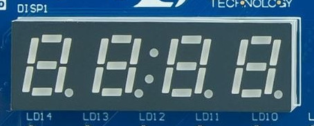
The Basys3 board contains a 4-digit, seven-segment display as shown below. This display can be used to display any information you desire, such as a counter value, register values, a timer, etc. In this week’s lab you will create a circuit to drive one digit of this display. Later in the semester, you will develop a module to drive all the four digits at once.
Before designing a seven-segment controller circuit, it is necessary to understand how the seven-segment display operates. You may want to review the “Basic I/O” section of the Basys3 Reference Manual to learn more about how the seven segment display is wired on the Basys3 board. As the name implies, a seven-segment display has seven discrete segments that can each be individually turned on to make a variety of different characters. Each of the seven segments are labeled with a letter as shown in the image below:
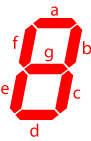
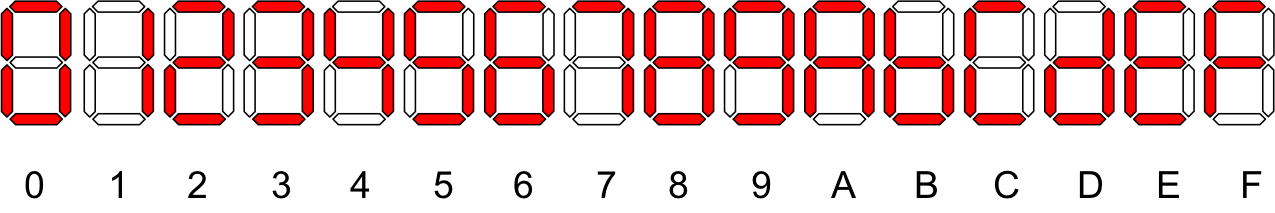
For example, the character “0” can be displayed on the seven-segment display by turning on segments a, b, c, d, e, f, and turning off segment g. Although any arbitrary combination of segments can be turned on, digital circuits are often created to display the 16 different characters representing any 4-bit value in hexadecimal. These characters are: 0, 1, 2, 3, 4, 5, 6, 7, 8, 9, A, B, C, D, E, and F. Each of these is shown in the image below.
Each segment of the seven-segment display is driven by an individual LED (light-emitting diode). The schematic diagram below shows these LEDs used by a seven-segment display. In addition to the seven segments for displaying a character, many displays include an eighth LED for the digit point (the dot to the bottom right of the seven segments). This is commonly abbreviated to DP as seen below. In this configuration, all eight LEDs share a common anode which enables the display. Each segment has its own cathode signal labeled CX where X represents the segment letter. For example, signal CA corresponds to the cathode signal for segment a.
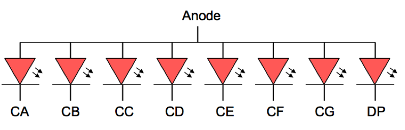
To turn on an LED, there must be a sufficient voltage drop from anode to cathode. That is, the anode needs to have a high voltage (‘1’) and the cathode has to have a low voltage (‘0’). Go back and read that last sentence again - what do you drive onto a cathode wire to turn a segment on? To display the character 0, the anode signal will have a high voltage, the cathode signals CA, CB, CC, CD, CE, and CF will have a low voltage, and the cathode signal CG will have a high voltage.
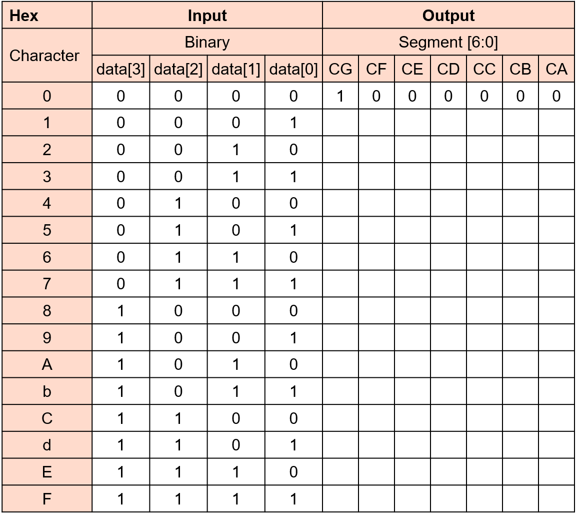
Before you can create a circuit to display these hexadecimal characters, you need to determine the value each cathode signal needs for each character. Fill out the decoder table below so that the segment outputs on each row will display the number given by that row’s hexadecimal character. Also included in this table is the binary representation of each hexadecimal character in the D columns. The first row of the table is completed and shows the segments that will be active for an input of 0. Carefully look at the top entry (which will display a ‘0’ digit) to make sure you understand. You will want to save this table as you will need it for Lab 7.
Decoder Table
After filling in the decoder table for a seven-segment display, answer the following questions in your laboratory report:
Provide the requested segment values from the decoder table.
Provide a logic equation for segment A (CA).
If you’re confused about how to make an equation for a segment, remember that a whole column represents an individual output. Simply pick the column for the segment as labeled in the table as a truth table output and read off the equation. On Learning Suite, you will only have to fill in a few sections of this table. But, make sure that your entire table is correct – it will make the rest of this lab much easier.
The Board’s 7 Segments
The seven-segment display on the Basys3 board has four unique digits as shown below. Each digit of the four-digit display has its own anode input (A0-A3). NOTE however, that there is a built-in inverter on each anode signal. Thus, to turn on any of the segments of a digit, its corresponding anode and cathode signals must both be driven LOW. The schematic of this four-digit, seven-segment display is shown below.
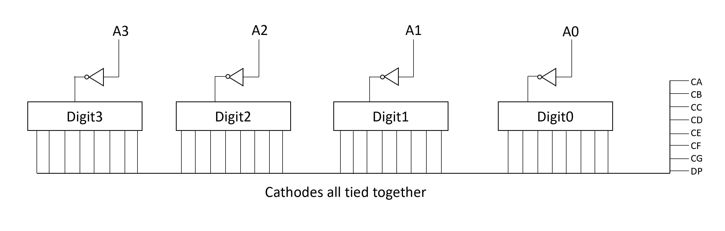
This four-digit, seven-segment display configuration is known as a common cathode arrangement because the cathode signals are shared among all four digits. If more than one anode signal is asserted low, the corresponding digits will have the same segments turn on because they are connected to the same cathode signals. While this significantly reduces the pin count, it makes it difficult to display different values simultaneously. Different values can be displayed by quickly switching between the various anode and cathode signals — the LEDs will flash so quickly your eye will see them as all being “on”. This is called “time-multiplexing” the digits. You will be given a time-multiplexing seven-segment display controller to use in future laboratory assignments. For example, to turn on only the right two digits of the four digit display, AN1 and AN0 must have a logic value of 0 and the other anode signals must have a logic value of 1.
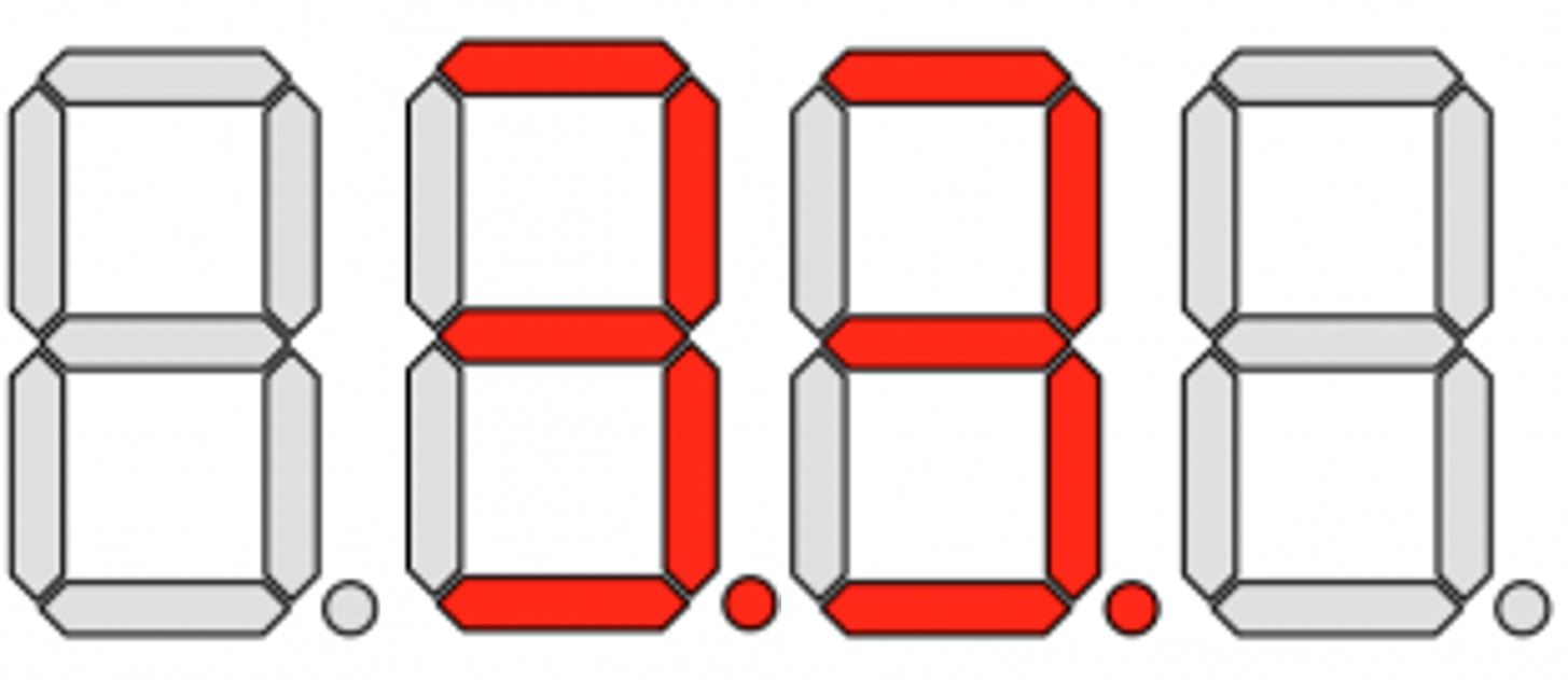
In the following example, two of the digits are turned on by setting their corresponding anode to zero. The other digits are off since their anode signals are set to one. In addition, the digit 3 is displayed based on which cathode signals have a logic 0. The digit point is also on since the cathode signal, DP, associated with the digit point is set to 0.
| A3 | A2 | A1 | A0 |
|---|---|---|---|
| 1 | 0 | 0 | 1 |
| DP | CG | CF | CE | CD | CC | CB | CA |
|---|---|---|---|---|---|---|---|
| 0 | 0 | 1 | 1 | 0 | 0 | 0 | 0 |
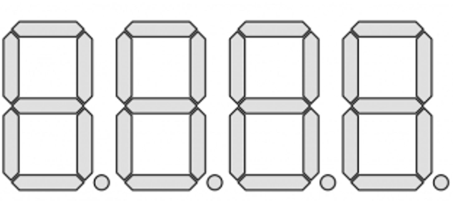
What would happen if all four anode control signals were set to a logic value of 0 simultaneously in the example above?
Determine what will be shown on the display with the following signal values.
| A3 | A2 | A1 | A0 |
|---|---|---|---|
| 0 | 1 | 0 | 1 |
| DP | CG | CF | CE | CD | CC | CB | CA |
|---|---|---|---|---|---|---|---|
| 1 | 1 | 1 | 1 | 1 | 0 | 0 | 0 |
Exercises
Exercise #1 - Seven-Segment SystemVerilog
In this exercise you will create a seven-segment decoder in a SystemVerilog module. You will create the logic for just one digit.
Create a new SystemVerilog file, seven_segment.sv, with the following module name and ports:
| Module Name: seven_segment | |||
|---|---|---|---|
| Port Name | Direction | Width | Function |
| data | Input | 4 | Data input to display on the seven-segment display |
| segment | Output | 7 | Cathode signals for seven-segment display (excluding digit point). segment[0] corresponds to CA and segment[6] corresponds to CG |
You will need to create seven different combinational logic circuits where each circuit drives one of the seven segments of the display. You will need to create each segment with a slightly different style of combinational logic. The list below describes which style to use for each of the segments.
- Segment A: Dataflow SV using an
assignstatement and a logical expression in ‘minterm’ SOP form - Segment B: Dataflow SV using an
assignstatement and a logical expression in ‘maxterm’ POS form - Segment C: Gate-level in minimized SOP form (use only gates!)
- Segment D: Use a look-up table
LUT4primitive (see below for details) - Segment E: Gate-level in minimized POS form
- Segment F: Dataflow SV using an
assignstatement and the?:(sometimes called the ternary) operator. - Segment G: Gate-level only using ‘nand’ gates
To make it easier to grade, provide the following comment before the logic for each segment of your code:
    /////////////////
    // Segment A
    /////////////////
Using the Look-Up Table (LUT) Primitive
The FPGA has a number of ‘primitive’ resources that you can instance directly in your design. One such primitive is a “Look up Table” or LUT that will perform a table lookup logic function where the look-up table contents can be specified by the designer. The LUT primitive you need to use for this design is the “LUT4” or the LUT with 4 inputs. A LUT with 4 inputs has 2^4=16 input combinations or rows in the lookup table. Details on this primitive can be found at the following document: LUT4.pdf.
The module definition for this primitive is:
module LUT4 #(parameter [15:0] INIT = 16'h0000) (
  output O,
  input I0,
  input I1,
  input I2,
  input I3
);
This primitive has four inputs: I0, I1, I2, and I3.
These inputs are the address inputs for the lookup table where I3 is the most significant and I0 is the least significant.
You will need to attach data[3] to I3, data[2] to I2, and so on.
The output, O, provides the output for the look-up table.
You will use this output to drive one of the segments of the seven segment display.
This primitive has a parameter, ‘INIT’, that specifies the contents of the look-up table. This parameter is 16-bits wide and contains one bit for each element of the look-up table. For example, if you want to implement an ‘AND’ function for the four inputs, the INIT parameter would be 16’h8000 (i.e., the function is only 1 when all inputs are 1). You will need to determine the INIT parameter for your seven segment logic. Note that when you use this primitive, it takes about 50 ns before it starts working properly. Make sure you simulate at least 50 ns of doing nothing before setting signals to get past this startup simulation time.
What is the INIT string if the LUT implements the function O = I0 & I1 | I2 & ~I3? Provide your response in the form: 16’hxxxx
The SystemVerilog example below demonstrates how to instance a single LUT into a design:
LUT4 #(.INIT(16'h8000)) seg_LUT (.O(seg), .I0(data[0]), .I1(data[1]), .I2(data[2]), .I3(data[3]) );
Include the file seven_segment.sv in your lab repository.
Exercise #2 - Seven Segment Decoder Verification
Once your seven segment decoder has been created, the next step is to verify its operation.
You will verify your seven-segment decoder circuit by a testbench named tb_sevensegment.v provided in the starter code.
Since your module includes an FPGA primitive ‘LUT4’ that is not a part of your design, you need to link the simulation library for this primitive.
Add the flag -L unisims_ver to the elaboration executable xelab in your Makefile.
In addition, you will need to add the flag --timescale 1ns/1ps to your xelab to set the timescale for the simulation (without it, you will get an error since the FDCE primitive has a timescale and your module does not).
Test your decoder interactively in GUI mode with this testbench to resolve syntax and behavioral problems in your design.
When you have resolved all the errors in the simulation, create a Makefile rule named sim_sevensegment that will run the simulation of your seven-segment decoder with the testbench.
This rule should generate a log file named sim_sevensegment.log.
Exercise #3 - Top-Level Design
You will create another SystemVerilog file as the ‘top-level’ design that instances your seven segment controller and adds logic to connect your controller to the display, buttons, and switches.
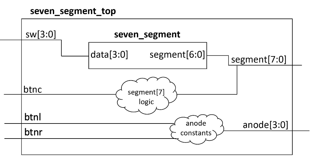
Begin this exercise by creating a SystemVerilog file named seven_segment_top.sv with the following module name and ports:
| Module Name: seven_segment_top | |||
|---|---|---|---|
| Port Name | Direction | Width | Function |
| sw | Input | 4 | Input from four switches to drive seven-segment decoder. |
| btnc | Input | 1 | Center button (will turn on digit point when pressed). |
| btnl | Input | 1 | Left button (will turn on all digits when pressed). |
| btnr | Input | 1 | Right button (will turn off all digits when pressed). |
| segment | Output | 8 | Cathode signals for seven-segment display (including digit point). segment[0] corresponds to CA and segment[6] corresponds to CG, and segment[7] corresponds to DP. |
| anode | Output | 4 | Anode signals for each of the four digits. |
The figure below demonstrates the structure of this top-level design. You will also create some additional logic in this top-level design.
Instance Seven-Segment Decoder Module
Begin your top-level module by instancing the seven-segment display module you created in the previous exercise.
Connect the four-bit switch input ports from your top-level design to the data inputs of your seven-segment display. Connect the 7 segment bits (segment[6:0]) from your seven-segment display outputs to the bottom bits [6:0] of the top-level segment output.
Digit Point
Your seven-segment decoder module drives seven of the eight cathode segment signals (segment[6:0]). The eighth segment signal (segment[7]) is used for the “digit point”. You need to create logic to turn on the digit point (DP or segment[7]). For this top-level design, we want to turn on the digit point when btnc is pressed. Create a logic circuit in your top-level module for the digit point based on the value of btnc. Remember that the cathode segment signals are turned on when the logic value of 0 is given. Use dataflow statements for your digit point signal logic.
Anode Signals
The last step of this top level Verilog design is to create the logic for the eight anode signals. Use dataflow statements for your anode signal logic. The logic for the anode signals should be designed to meet the following specifications:
- When no buttons are pressed, turn on only the rightmost digit, digit 0 (corresponding to anode[0]).
- When the left button is pressed, btnl, turn on all 4 digits. All 4 digits will display the same value as dictated by the switches and btnc for DP.
- When the right button is pressed, btnr, turn off all 4 digits (including digit 0). Note that this condition has lower priority than the previous condition. If both the right and left buttons are pressed at the same time, all digits should be turned on as described in the previous condition.
Note that your center button does not affect your anodes at all - it only affects segment[7]. Do not include the center button in your logic for the anodes.
In your top level design, the logic for anode[0] signal (driving digit 0) will be different from the logic for the anode[3:1] signals (driving digits 1-7). Since the logic for the anode signals anode[3:1] are all the same, it is best to use one signal to drive all of them.
Include the file seven_segment_top.sv in your lab repository.
After completing your top-level design, simulate the design with a Tcl script named sim_seven_segment_top.tcl.
Include the following in your Tcl script:
- Test all 16 input combinations for the seven segment display
- Test the function of the three buttons on the digit point, and anode signals.
After simulating and debugging your design, create a screenshot of your simulation waveform of the top-level signals and save the image in a file named
sim_seven_segment_top.png.
Include the file sim_seven_segment_top.tcl and sim_seven_segment_top.png in your lab repository.
Exercise #4 - Synthesis
Create an XDC file for your top-level design to map the top-level ports to pins on the Basys3 board.
Create a Makefile rule named synth that runs the synthesis script and generates a log named synthesis.log and a ‘.dcp’ file named seven_segment_synth.dcp.
Carefully review the synthesis log to make sure there are no Warnings.
How many total LUT resources are used by the design? (add up all the LUT* resources)
How many total IBUF resources are used by the design?
How many total OBUF resources are used by the design?
Exercise #5 - Implementation and Download
Proceed to the design implementation step by creating a Makefile rule named implement that performs the implementation step.
This rule should generate a log named implement.log, a .dcp file named seven_segment.dcp, a bitfile named seven_segment.bit, and a utilization report named utilization.rpt.
Carefully review the log to make sure there are no Warnings.
How many ‘Slice’s are used by the design from the utilization report?
How many ‘Bonded IOB’ resources are used from the design from the utilization report?
After successfully implementing your design, view the design implementation as described in the Viewing FPGA Design Layout tutorial.
Select the ‘seg_LUT’ element used to implement ‘segment D’ of your seven segment display controller and zoom into this look-up table.
Take a screenshot of this lookup table in the design layout view and name this screenshot segment_lut.png.
Include the file segment_lut.png in your lab repository.
Final Pass-Off:
- Required Files
seven_segment.svseven_segment_top.svsim_seven_segment_top.tclsim_seven_segment_top.pngsegment_lut.png
- Required Makefile ‘rules’
sim_sevensegment: requiresseven_segment.sv; generatessim_sevensegment.logsynth: requiresseven_segment.sv,seven_segment_top.sv; generatessynthesis.log,seven_segment_synth.dcpimplement: requiresseven_segment_synth.dcp; generatesimplement.log,seven_segment.dcp,seven_segment.bit,utilization.rpt
Answer the final two questions in your laboratory report:
How many hours did you work on the lab?
Provide any suggestions for improving this lab in the future