Table of Contents
In this lab you will implement a two’s complement binary adder and an overflow detector in a hierarchical design and demonstrate the ability to perform binary addition and subtraction and overflow detection.
«span style=”color:red;”>The average time to complete this lab is 4.6 hours.</span>
Learning Outcomes
- Demonstrate understanding of two’s complement addition, subtraction, and overflow detection
- Develop a hierarchical design with three levels of hierarchy
- Validate the circuit with a testbench
Preliminary
In this preliminary exercise, you will work through some binary arithmetic examples. Answer the following questions to demonstrate your understanding of two’s complement representation, sign extension, negation, addition, subtraction, and overflow detection. You may want to refer to Chapter 3 of the textbook specifically as you complete this preliminary work.
Determine the decimal value for the following eight-bit two’s complement binary numbers: (See Section 3.3)
10000100
00011001
Extend each of the following numbers to nine bits using sign-extension. Include leading zeros in the binary result: (See Section 3.3.1)
10000100
00011001
Negate each of the following eight-bit two’s complement numbers. Include leading zeros in the binary result: (See Section 3.3.2)
10000100
00011001
Overflow can be detected by inspecting the sign bit of the operands and the result. The sign bit is the MSB. If the sign bit of the two operands are different, then overflow cannot occur. If the sign bit of the result is opposite the two operands, two’s complement overflow has occurred.
Perform addition with the following eight-bit two’s complement numbers. Include leading zeros in the binary result. Indicate if overflow occurs with a ‘#’ sign at the beginning of the 8-bit result: (See Sections 3.3.3 and 3.5.1)
1)   10000100
   + 01100100

2)   01111111
   + 10011001

3)   01111111
   + 01100111

4)   00011010
   + 01001001

5)   11100110
   + 10110111

6)   10000100
   + 10011001
Subtraction can be performed with an adder circuit if the second operand is inverted before the operation and the carry-in is set to one. This method is equivalent to negation of the second operand followed by addition. In the following cases, you should negate the second number and then use two’s complement addition to calculate the result.
Perform subtraction with the following eight-bit two’s complement numbers. Include leading zeros in the binary result. Indicate if overflow occurs with a ‘#’ sign at the beginning of the 8-bit result: (See Sections 3.3.2, 3.3.3, and 3.5.1)
1)   10000100
   - 01100100

2)   01111111
   - 10011001

3)   01111111
   - 01100111

4)   00011010
   - 01001001

5)   11100110
   - 10110111

6)   10000100
   - 10011001
Exercises
Exercise #1 - 8-bit Binary Adder
In this exercise, you will create an 8-bit two’s complement full adder for implementing arithmetic. You will do this with two SystemVerilog files:
- A single-bit full adder module (
FullAdd.sv) - A multi-bit adder that combines eight single-bit adders (
Add8.sv)
This is a classical hierarchical design: you will create a simple 1-bit full adder module, and you will then create a new module and instance 8 of your 1-bit adders inside it to build up your circuit.
1-bit Full Adder
Create an empty SystemVerilog file named FullAdd.sv and add the following ports to this module as described in the table below:
| Module Name: FullAdd | |||
|---|---|---|---|
| Port Name | Direction | Width | Function |
| a | Input | 1 | ‘a’ operand input |
| b | Input | 1 | ‘b’ operand input |
| cin | Input | 1 | Carry in |
| s | Output | 1 | Sum output |
| co | Output | 1 | Carry out output |
Once you have created the empty module with the ports outlined above, create the single-bit full adder cell as shown in Figure 9.2 of the text. Like the diagram, your circuit should include a 3-input XOR gate, three 2-input AND gates, and a 3-input OR gate. Note that you must use structural SystemVerilog to create this full adder cell. Although there are easier ways to create adder circuits using dataflow SystemVerilog, you are required to use structural SystemVerilog for this lab.
Make sure you follow the class’s SystemVerilog Coding Standards. In particular, pay attention to the following standards: S14, S15
Include the file FullAdd.sv in your lab repository.
Once you have created your circuit, simulate the full adder by testing all possible input conditions.
Create a Tcl file named sim_FullAdd.tcl to provide the stimulus for this simulation.
The Tcl code below simulates two of the eight conditions.
# Simulate a=0, b=0, cin=0 for 10 ns
add_force a 0
add_force b 0
add_force cin 0
run 10 ns

# Simulate a=1, b=1, cin=1 for 10 ns
add_force a 1
add_force b 1
add_force cin 1
run 10 ns
Include the file sim_FullAdd.tcl in your lab repository.
8-Bit Adder
As mentioned above, this lab will involve hierarchy. This is covered in-depth in Chapter 11, but will be briefly explained here.
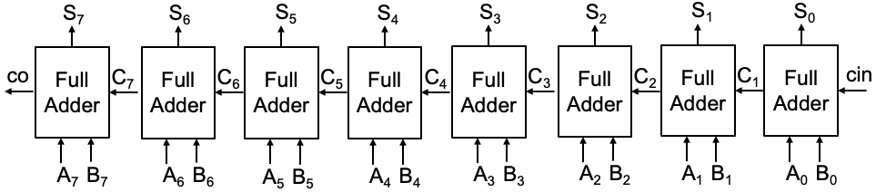
A circuit with hierarchy is a circuit that contains modules within modules. In many complex digital logic circuits there are many levels of hierarchy. In this circuit you will have three levels of hierarchy - your FullAdd, your Add8, and a top-level module. For this step you will create the Add8 module which will instance 8 FullAdd modules. Program 11.1.1 in your textbook gives an example of instancing modules.
Begin the creation of an 8-bit ripple-carry adder by making a new SystemVerilog file named Add8.sv and add the following ports as shown in the table below:
| Module Name: Add8 | |||
|---|---|---|---|
| Port Name | Direction | Width | Function |
| a | Input | 8 | ‘a’ operand input |
| b | Input | 8 | ‘b’ operand input |
| cin | Input | 1 | Carry in |
| s | Output | 8 | Sum output |
| co | Output | 1 | Carry out of last stage |
After creating the empty module, create the needed local wires (you will need some, figure out where). For example, the carry signals that go between the various adder stages is one place where you will need them. You could declare each such carry signal individually with names like c3, c4, … Or, you could declare a multi-bit wire and use indexing with square brackets to get at the various bits. It is your choice.
Insert 8 instances of your FullAdd module into your Add8 module (as described in Section 9.1 of the textbook and as shown in the figure below). You should use the .port(wire) way of mapping ports on instances to your wires (see Program 11.1.2 in the textbook). Note that the co (1 bit) output of your Add8 is the carry-out of the last FullAdd instance.
Include the file Add8.sv in your lab repository.
Simulate the behavior of your 8-bit adder by creating a Tcl script named sim_Add8.tcl.
Provide at least one input condition for each of the following cases to test your adder.
You could use the examples for addition in the Preliminary section above.
Note that this 8-bit adder does not implement overflow detection.
You will have to examine the simulation output to determine if there is overflow.
- Add a positive binary number to a negative binary number.
- Add two positive binary numbers without overflow.
- Add two positive binary numbers with overflow.
- Add two negative binary numbers without overflow.
- Add two negative binary numbers with overflow.
Rather than assigning each bit of an input with a single Tcl command, you can assign all 8 bits of an input with a single “add_force” command as shown in the following example:
add_force a 11000101
Include the file sim_Add8.tcl in your lab repository.
Exercise #2 - Top-Level Design
For this exercise you will create a top-level design named arithmetic_top.sv that instances your 8-bit adder and connects your adder to a button, the switches and LEDs.
Both operands to the adder will be interpreted as two’s complement numbers.
Begin your design by creating a top-level module with the following name and ports.
| Module Name: arithmetic_top | |||
|---|---|---|---|
| Port Name | Direction | Width | Function |
| sw | Input | 16 | Switches (sw[15:8] = ‘b’, sw[7:0] = ‘a’ operand) |
| btnc | Input | 1 | Center button (subtract when pressed) |
| led | Output | 9 | LEDs (led[8] = overflow, led[7:0] = sum) |
NOTE: the name of the module and the ports are crucial – use what is in the table above.
The reason for using the exact names is that the testbench you will use below to prove your circuit works relies on the top-level module being called ‘arithmetic_top’ and on the ports having the specified names.
A block diagram of the overall design is shown below. It has an input signal called sub (refer to Figure 9.4). The top-level circuit will perform addition when sub is 0 and subtraction when sub is 1. The center button (btnc) serves as the sub signal. When btnc = 1’b0, addition is performed, and when btnc = 1’b1, subtraction is performed. The sub signal must be connected to the carry-in input of the Add8 adder.
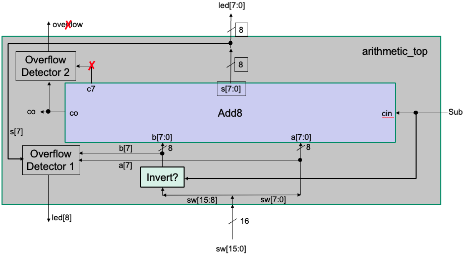
Inside your top-level module, the carry-out of the Add8 adder is not used, but you do need to connect something to it. So, declare a local signal for it and connect it to the carry-out of the adder. Do not connect this local signal to anything else — the synthesis tool will recognize that it is unused and discard it without issues.
The input ‘btnc’ controls the inversion of the b input to the adder. When performing subtraction (btnc = 1’b1), the bits of b must be inverted before being passed to the adder.
As can be seen from the block diagram, the top-level module will also contain logic to implement overflow detection. The output from the overflow detector is connected to led[8].
Overflow can be detected by looking at the signals a[7], b[7], and s[7]. Overflow occurs in one of the following cases:
- Both inputs are positive (a[7] = 0, b[7] = 0) but the result is negative (s[7] = 1).
- Both inputs are negative (a[7] = 1, b[7] = 1) but the result is positive (s[7] = 0).
This overflow logic can be expressed in a Boolean equation:
overflow = (a[7]' b[7]' s[7]) + (a[7] b[7] s[7]')
You must use built-in gates (e.g., not, and, or) to implement this circuit as part of the top-level module.
Key Implementation Notes:
- The
btncsignal directly controls both the carry-in of the adder and the inversion of b. - The sum output (
s) of the adder is assigned toled[7:0]. - The overflow detection output is assigned to
led[8]. - The unused carry-out signal from the Add8 adder should be connected to a local signal, which will be discarded during synthesis.
Include the file arithmetic_top.sv in your lab repository.
Viewing Hierarchy in Vivado
After completing your top-level design, you can view the hierarchy of your design in Vivado. Follow the Viewing Hierarchy Tutorial to learn how to generate a schematic of your design and navigate the hierarchy of the design. After viewing this tutorial, create a schematic of your top-level design and expand the hierarchy as follows:
- Press “+” on the Add8 cell so you can see the top-level and the contents of the Add8 on the same schematic
- Press “+” on the first ‘FullAdd’ cell so you can see the top-level, ‘Add8’, and one ‘FullAdd’ on the same schematic
- Zoom out enough so you can see all three levels of hierarchy on the same schematic (don’t worry about missing small text details)
Take a screenshot of this schematic and name it hierarchy.png and include it in your lab repository.
Include the file hierarchy.png in your lab repository.
Exercise #3 - Simulating with a Testbench
When you have completed your top-level design and removed all syntax errors, simulate your design manually using Tcl scripts to convince yourself that your circuit is working properly (the Tcl scripts are not required for your submission).
Once you believe your circuit is working properly, test your design with the testbench file tb_arithmetic.sv that has been included in your starter code.
You may want to refer to the Simulating with Testbenches tutorial introduced in lab 3 to refresh your memory on how to simulate with a testbench.
When you have debugged your module, and it is passing the testbench tests, create a Makefile rule named sim_testbench that runs the testbench and generates a log named testbench.log.
This testbench will be run as part of your passoff script and the testbench will be reviewed by the TAs as part of the lab grading process.
What time does the simulation start? (i.e., Starting simulation at time X ns)?
What time is the simulation done (in ns)?
How many test cases are applied in the testbench?
Exercise #4 - Synthesize, Implement and Download
Begin this exercise by creating and adding an XDC constraints file.
You can name it whatever what you want, but you will need to include it in your repository and name it appropriately in the synthesis script (this file will not be graded, but your design will not work if it is incorrectly created).
Your XDC file should include an entry for each of the ports in the top-level design.
Consider copying the master XDC file for the Basys3 board in the ./resources directory.
With a xdc file, create a synthesis tcl script that performs the synthesis step.
You can name this script whatever you want, but you must include it in your repository.
Create a Makefile rule named synth that runs the synthesis script and generates a log named synthesis.log and a ‘.dcp’ file named arithmetic_top_synth.dcp.
Carefully review the synthesis log to make sure there are no Warnings.
How many total LUT resources are used by the design? (add up all the LUT* resources)
How many total IBUF resources are used by the design?
How many total OBUF resources are used by the design?
After successfully synthesizing your design, view the post-synthesis schematic from the ‘.dcp’ file created during the synthesis step (see the Vivado Schematic Tutorial). Take a screenshot of this schematic and name it ‘post-schematic.png’.
Include the file post-schematic.png in your lab repository.
You will notice that unlike the pre-synthesis schematic you created in an earlier exercise, this schematic is “flat” meaning that there is no longer any hierarchy. All levels of hierarchy have been flattened into a single netlist using FPGS primitives.
Proceed to the design implementation step by creating a Makefile rule named implement that performs the implementation step.
This rule should generate a log named implement.log, a .dcp file named arithmetic_top.dcp, a bitfile named arithmetic_top.bit, and a utilization report named utilization.rpt.
Carefully review the log to make sure there are no Warnings.
How many ‘Slices’ are used by the design from the utilization report?
How many ‘Bonded IOB’ resources are used from the design from the utilization report?
Download your design to the board and make sure your design operates properly. The TAs will be building your design and checking it themselves so make sure it works before submitting your lab.
Final Pass-Off
Make sure you have the following required files in your repository and Makefile rules implemented before you pass off this lab. Refer to the passoff tutorial for questions about the passoff process.
What to commit: As a general rule of thumb, commit any files that you create yourself (e.g., .sv, .png, .tcl, etc.) and ignore and clean any generated files (e.g., .log, .dcp, .bit, etc.).
- Required Files
FullAdd.svsim_FullAdd.tclAdd8.svsim_Add8.tclarithmetic_top.svhierarchy.pngpost-schematic.png
- Required Makefile ‘rules’
sim_testbench: requiresFullAdd.sv,Add8.sv,arithmetic_top.sv,tb_arithmetic; generatestestbench.logsynth: requires<synthScriptName>.tcl,FullAdd.sv,Add8.sv,arithmetic_top.sv,<constraintsFileName>.xdc; generatessynthesis.log,arithmetic_top_synth.dcpimplement: requiresimplement.tcl,arithmetic_top_synth.dcp; generatesimplement.log,arithmetic_top.dcp,arithmetic_top.bit,utilization.rpt
Answer the final two questions in your laboratory report:
How many hours did you work on the lab?
Provide any suggestions for improving this lab in the future