Table of Contents
In this lab you will implement several logic functions using the SystemVerilog HDL (Hardware Description Language). You will simulate your SystemVerilog designs and synthesize them into circuits. You will then download the resulting circuit data onto the Basys3 board, so you can test your design in hardware.
The average time to complete this lab is 3.1 hours.
Learning Outcomes
- Describing circuits using SystemVerilog.
- Learn how to simulate with waveform viewers.
Preliminary
The primary activity of this lab is to create your first SystemVerilog module. You will then simulate it, synthesize it, and implement it on the Basys3 board. Review Chapter 8 of the textbook (you will need to be familiar with SystemVerilog before starting this lab) and answer the questions below.
Match the SystemVerilog language style with the code
Which of the following examples generates a 3-input AND gate: D = A * B * C
Which of the following examples is the proper syntax for a module?
The order of ‘gate’ statements in structural SystemVerilog does not matter
How can you add comments in SystemVerilog? (select all that apply)
Exercises
Exercise #1 - Implement Logic Functions in Structural SystemVerilog
In this exercise you will create the structural SystemVerilog description of several logic functions. Note that you must use structural SystemVerilog rather than Dataflow SystemVerilog to complete this assignment. Follow the steps below to begin this exercise.
1. Create an empty text file named logic_functions.sv and add it to your lab repository.
2. Start your file by creating a header in your SystemVerilog file that conforms to this class’s SystemVerilog Coding Standards. In addition to the general coding standards, the SystemVerilog coding standards you should pay close attention to include: S2, S6, S7, S8, S10, S11, S15, S21, and S22
3. Define a module named “logic_functions” with the ports listed below. Make sure to match everything described below exactly (including the port names). NOTE: if you are fuzzy on module declarations, consult the textbook. In particular, review Sections 8.3, 8.4, and 8.6.1 in the textbook.
| Port Name | Size (bits) | Direction |
|---|---|---|
| A | 1 | Input |
| B | 1 | Input |
| C | 1 | Input |
| O1 | 1 | Output |
| O2 | 1 | Output |
| O3 | 1 | Output |
| O4 | 1 | Output |
4. Create the logic for the following functions using structural gates. There is no reason to get creative - just copy the structure and syntax (including indentation) of the code examples in the book sections noted.
-
O1: O1 = AC+A’B
-
O2: O2 = (A+C’)(BC)
-
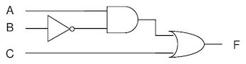
O3: The logic function below (implement the gates as shown):
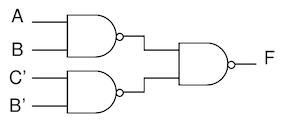
- O4: The logic function below (implement the gates as shown):
If these functions require intermediate signals (signals that are not module ports), you will need to declare them using the ‘logic’ keyword (see text for details).
Also, choose meaningful names or (probably better yet) put a comment above them to tell what they are used for.
You do not need to minimize these functions, just implement the logic functions directly using basic gates (AND, NAND, OR, NOR, NOT, etc.).
Edit your SystemVerilog file until there are no syntax errors (use the xvlog command to check for syntax errors).
Do not use the default_nettype none directive at the beginning of your file as suggested in 8.6.1 of the textbook.
Include the file logic_functions.sv in your lab repository.
Exercise #2 - Simulation
In this exercise you will simulate your new module to make sure it is operating correctly. You may want to review the Vivado Command Line Simulation Tutorial from the previous lab to remind yourself how to perform logic simulation.
1. Perform analysis and elaboration on your module
2. Run xsim in GUI mode
3. Create a .tcl simulation script named sim_logic.tcl to simulate all possible input combinations of your logic functions.
The following .tcl code snippet demonstrates one way to simulate two of the eight input combinations.
In your own .tcl file you will need to make sure to test all possible input combinations.
# Simulate A=0, B=0, C=0 for 10 ns
set_value A 0
set_value B 0
set_value C 0
run 10 ns

# Simulate A=0, B=0, C=1 for 10 ns
set_value A 0
set_value B 0
set_value C 1
run 10 ns
Include the file sim_logic.tcl in your lab repository.
4. Compare the resulting waveform with a truth table for your four functions.
Verify that your simulation outputs match the expected outputs.
If there are errors, fix your SystemVerilog file and simulate again until your circuit operates as intended.
Once you have verified that your simulation is working correctly, create a screenshot of your simulation waveform and name it sim_logic.png.
Make sure your waveform includes all possible input combinations.
Include the file sim_logic.png in your lab repository.
Exercise #3 - Testbench Simulation
Using Tcl files in an interactive simulation environment is a good way to find errors early in the simulation phase. However, it is difficult to fully test complex digital circuits with Tcl files. A more thorough way to test your digital circuit is to use a special SystemVerilog module called a testbench. In this exercise you will be given a SystemVerilog testbench file that will test your circuit. You will also be using testbench files in all future labs.
Follow the Simulating with Testbenches tutorial to learn how to simulate your design with a testbench.
When your testbench is operating correctly, create a Makefile simulation rule named sim_tb that runs the testbench simulation and generates a log file named testbench.log.
Note that the Simulating with Testbenches tutorial commands use the --nolog flag that you will need to replace with -log testbench.log.
Answer the following questions in your laboratory report:
What is the time in nano seconds in which the simulation ends?
What are the values of A,B,C at time 140ns in the testbench simulation?
Exercise #4 - Synthesis
During this exercise you will translate your SystemVerilog HDL file into an actual digital circuit that can operate on the FPGA device. You will follow the same steps as in the previous lab to synthesize and implement your design. You may want to refer to the tutorials from the previous lab to remind yourself how to perform these steps. The instructions in this lab will provide reminders of the steps you need to take.
Pre-Synthesis Schematic
Create a pre-synthesis schematic of your circuit as you did in lab01.
See the Vivado Schematic Tutorial for a reference on how to do this.
Take a screenshot of the schematic and save it in the file pre-synth-schematic.png within your repository
Include the file pre-synth-schematic.png in your lab repository.
How many gates are shown in this schematic?
Creating a Constraints File
The first step in implementing your design is to create a constraints file, or .xdc (Xilinx Design Constraints) file.
This file is used during the synthesis and implementation steps to map the inputs and outputs of your design to the physical pins on the FPGA.
In the tutorial for the previous lab, an .xdc file was create for you.
For this lab, you will need to create an .xdc file named logic_functions.xdc.
Review the principles of creating an XDC file in the Creating XDC files tutorial.
The table below shows the mapping we will use for this module.
| Port Name | Pin | Basys3 |
|---|---|---|
| A | W16 | Switch 2 (SW2) |
| B | V16 | Switch 1 (SW1) |
| C | V17 | Switch 0 (SW0) |
| O1 | V19 | LED 3 (LD3) |
| O2 | U19 | LED 2 (LD2) |
| O3 | E19 | LED 1 (LD1) |
| O4 | U16 | LED 0 (LD0) |
For example, this table indicates that the “A” input to your logic circuit should be mapped to pin “W16” of the FPGA on the Basys3 board. The table also indicates that the “W16” pin is attached to Switch 2 on the board. Your constraints file should have seven different constraint commands, one for each of the inputs and outputs of your circuit.
Include the file logic_functions.xdc in your lab repository.
Logic Synthesis
The next step in the process is to ‘synthesize’ the SystemVerilog files into a format that can be used within the FPGA.
Create a Tcl script named synth_logic.tcl that will run the synthesis process and a Makefile rule named synth_logic that will run the Tcl script in batch mode.
The rule should also create a file named synth_logic.log that contains the output of the synthesis process and the Tcl script should create a file named logic_functions_synth.dcp that contains the checkpoint file for your synthesized design.
Make sure your synthesis Tcl script includes the source ../resources/messages.tcl command to set the message severity levels for the synthesis tool.
You may need to refer to the Vivado Command Line Synthesis Tutorial to help you complete this step.
During the synthesis process you may encounter synthesis warnings or errors from the synthesis tool. You must review these warnings and errors and make sure that you do not have ANY synthesis warnings before proceeding to the next step. Review the synthesis log file and answer the following questions:
How many total LUT resources are used by the design? (add up all the LUT* resources)
How many total IBUF resources are used by the design?
How many total OBUF resources are used by the design?
After successfully generating a ‘.dcp’ file from the synthesis step, generate a schematic of the post-synthesis design (see the Vivado Schematic Tutorial).
Take a screenshot of this schematic and name it post-synth-schematic.png.
Remember that the ‘schematic’ view is the view that shows the actual cells (in yellow) wired up together.
This is different from the ‘implementation’ view that is a view of the FPGA layout with your design.
Include the file post-synth-schematic.png in your lab repository.
Exercise #5 - Implementation and Download
After the design has been successfully synthesized, perform the “Implementation” step to map the synthesized design onto the FPGA.
You may want to refer to the Vivado Command Line Implementation Tutorial to remind you how to do this.
Create a Tcl script named implement_logic.tcl that will run the implementation process and a Makefile rule named implement_logic that will run the Tcl script in batch mode.
The rule should also create a file named implement_logic.log that contains the output of the implementation process, and the Tcl script should generate a file named logic_functions.bit that contains the bitstream for your synthesized design, a file named logic_functions.dcp that contains the final design checkpoint, and a file named utilization.rpt that contains the utilization report for your design.
It is often helpful to view a “schematic” or structural representation of the circuit you are designing. In this exercise you will be creating three different schematics: a pre-synthesis schematic, a post-synthesis schematic, and a post-implementation schematic. Each of these schematics will be different and represent your design in different stages of the design flow. You will use the Vivado tools to generate these schematics.
After successfully creating a bitstream file (and .dcp file), you can view the internal design of the FPGA.
Follow the instructions in the Viewing FPGA Design Layout tutorial.
With the design layout window open, zoom into the LUT resources used by your design and enable the display of the routing resources.
Take a screenshot of this view and name the image implementation.png within your repository.
Include the file implementation.png in your lab repository.
The final step involves downloading the bitstream file to the Basys3 board and testing the operation of the design on the board. Follow the steps described in the Bitstream Download Tutorial to download the bitstream file to the Basys3 board. Test all four functions of your circuit on the board to make sure that it works correctly. When you are convinced that your circuit is correct, proceed to the final pass off.
Final Pass-Off
Make sure you have the following required files in your repository and Makefile rules implemented before you pass off this lab. Refer to the passoff tutorial for questions about the passoff process.
What to commit: As a general rule of thumb, commit any files that you create yourself (e.g., .sv, .png, .tcl, etc.) and ignore and clean any generated files (e.g., .log, .dcp, .bit, etc.).
- Required Files
logic_functions.svsim_logic.tclsim_logic.pngpre-synth-schematic.pnglogic_functions.xdcpost-synth-schematic.pngimplementation.png
- Required Makefile ‘rules’
sim_tb: requireslogic_functions.sv, generatestestbench.logsynth_logic: requiressynth_logic.tcl,logic_functions.xdc, generatessynth_logic.log,logic_functions_synth.dcpimplement_logic: requiresimplement_logic.tcl,logic_functions_synth.dcp, generatesimplement_logic.log,logic.dcp,logic.bit,utilization.rpt
Answer the final two questions in your laboratory report:
How many hours did you work on the lab?
Provide any suggestions for improving this lab in the future