Table of Contents
In this lab you will prepare your lab GitHub repository and familiarize yourself with the Basys3 FPGA development board that you will use throughout the semester.
Each laboratory has a write-up page (this is one of them) that provides the detailed instructions for completing the laboratory assignment. You will need to read the laboratory write-up and refer to it frequently to successfully complete the lab.
The average time to complete this lab is 3.4 hours (W25)
Learning Outcomes
Each laboratory assignment starts by summarizing the expected learning outcomes for the laboratory exercise. The learning outcomes for this lab are:
- Understand how laboratories are completed in ECEn 320
- Understand how to complete and submit lab reports
- Create a ECEN 320 GitHub classroom repository and initialize it with the class starter code
- Become familiar with the BASYS3 FPGA board and the process of downloading a bitstream file to the board
This laboratory assignment will involve a lot of tutorials to help you get oriented to the class lab, tools required for the lab, and process for submitting labs.
Preliminary
Each laboratory assignment contains a “Preliminary” section that involves tutorials, training, and reading that will help you get started with the lab before you show up for the lab assignment. You are encouraged to read and start the laboratory preliminary before you show up to the lab. Students who complete the preliminary section of the lab before the laboratory section will be far ahead of other students and have access to the TAs before the TAs get too busy. This preliminary section will guide you through the laboratory completion and submission process and introduce you to the BYU ECEN Digital Laboratory.
Basys3 Board
You will need a Basys3 FPGA board to complete the laboratory assignments in this class. You can purchase a board from the ELC Shop or online. You will also need to obtain a Micro-USB cable to connect the Basys3 board to your computer (this cable does not come with the Basys3 board).
Laboratory Completion Instructions
Begin this preliminary by carefully reading through the instructions for completing lab assignments. After reading these instructions, answer each of the following questions in your lab report (i.e., Learning Suite).
What portion of your composite laboratory grade is the “Lab Report” component?
How do you submit a laboratory report in this class?
When are laboratory lab reports due?
Are late lab reports accepted?
How are files submitted for the passoff section of the lab?
When are laboratory Passoffs due?
Are late lab passoffs accepted?
Teams Lab Channel
There will be a dedicated channel in the class Teams workspace for each laboratory assignment. Click on this link to join the class Teams if you have not already done so. You will automatically be added to this channel when it is created. This Teams channel is used to provide updates or clarification on the lab as problems are discovered. Students are encouraged to ask questions about the lab on this channel and provide answers to other students. The TAs and instructor will monitor this channel and provide responses as needed.
What is the preferred way to communicate with the TAs and instructor for laboratory assignments?
ECEN Digital Lab
You will use the computers in room 423 EB to access the software for designing digital hardware. To access these computers, you will need an active CAEDM account. Request a CAEDM account if you do not already have one. When in this room (423 EB), you are required to follow all CAEDM policies. Review these policies and answer the following question:
Which activities are acceptable in the Digital Lab?
These computers run the Linux operating system, and it is expected that you are able to comfortably navigate and work within the Linux command line shell. The following resources can be used to review your Linux skills:
You will be creating and editing a lot of text files as you complete the laboratory assignments in this class. It is strongly recommended that you use the ‘vscode’ text editor to create and edit these files. The ‘vscode’ text editor is available on the CAEDM computers and contains a number of extensions that will help you in your text editing. Review the following VSCode Tutorial to help you get started using this editor. You will be creating several text files as part of this laboratory, and you are encouraged to do this in VSCode.
Exercise #1 - GitHub Classroom Repository
GitHub will be used extensively in this class for submitting and grading your laboratory files. You will be required to create a GitHub classroom repository to store your laboratory files. Carefully read and follow the instructions in the GitHub Setup Guide to set up your class repository and import the initial class starter code.
What is the Web URL of your github repository?
There is a file in the ‘lab01’ directory named ‘color.txt’. What color is listed in this file? (you can access this file from the GitHub web interface)
Once you have an initial classroom repository, you will need to ‘clone’ the repository to your drive on your CAEDM drive and possibly on other computers such as your personal laptop. Carefully read and follow the instructions in the GitHub Clone Guide to clone your class repository onto a remote computer.
What is the purpose of the ‘startercode’ remote repository that you attached to your repository?
Is it possible to check out your classroom repository on more than one computer?
You will need to become familiar with using GitHub for submitting your laboratory files.
To learn some of the most basic functions of Git, complete the GitHub Basic Tutorial.
As part of this tutorial you will create a file named aboutme.txt and commit it to your repository (instructions on what should be included in this file are described in the tutorial).
You are encouraged to use the ‘vscode’ text editor to create this file.
Make sure you read the instructions carefully as there are two parts involved with creating this file (students frequently skip the second part and fail to add all the required information in the aboutme.txt file).
Include the file aboutme.txt in the ‘lab01’ directory of your repository.
Note: This green text above indicates that the aboutme.txt must be included in your passoff GitHub repository when you submit your lab.
This file should contain the information requested during the tutorial and will be reviewed by the TAs.
After reading the instructions on GitHub, answer each of the following questions in your lab report to demonstrate your understanding of Git and its use in the class.
What is the purpose of each of the following ‘git’ commands? ‘status’, ‘add’, ‘commit’, ‘push’, ‘fetch’, ‘pull’, and ‘merge’
Exercise #2 - Lab Makefiles
Completing the labs in ECEN 320 will require you to create a Makefile and provide lab-specific ‘rules’ to perform various actions on your lab submissions.
For example, you will create Makefile rules to build digital circuit projects, simulate circuit designs, and analyze design results.
You should have a basic understanding of what Makefile are and how to create them.
The following resources will help you learn more about Makefile if you are rusty:
Begin by creating a file named Makefile in your lab directory and add a rule about that ‘cat’s’ the aboutme.txt file created in the previous exercise:
about:
    cat aboutme.txt
When you type make about on the command line, your aboutme.txt file will be printed on the screen.
Note that this rule is necessary to successfully complete the passoff script described at the end of the lab.
Lab Makefile Rules
Unlike the previous example, most makefile rules will involve creating new files.
For this exercise you will create a number of makefile rules to create new files that perform a variety of operations on the aboutme.txt file created above.
You may need to look up details about various Unix commands to perform the functions described below.
Note that these rules must operate correctly on the computers in the digital lab.
Create each of the following Makefile rules described below.
reverse
Create a makefile rule named reverse that creates a new file named reverse.txt in which the text of each line in the aboutme.txt has its characters reversed (i.e., the first line of this new file as the last character first, the second to last character second, and so on).
Consider using the Unix ‘rev’ command.
upper
Create a makefile rule named upper that creates a new file named upper.txt in which the text of the aboutme.txt is all in upper case.
Consider using the Unix ‘sed’ command.
lineno
Create a makefile rule named lineno that creates a new file named lineno.txt that prepends the line number to each line in the aboutme.txt file.
Consider using the Unix ‘nl’ command.
bottom
Create a Makefile rule named bottom that creates a new file named bottom.txt that contains the last 3 lines of the aboutme.txt file.
Consider using the Unix ‘tail’ command.
At this point you should have a Makefile with the following rules: about, reverse, upper, lineno, and bottom.
The lab passoff script will check to make sure that all of these rules exist.
Temporary Files
The makefile rules you created above will create new files when the corresponding rule is executed.
These are temporary files that should not be committed into your repository.
You will notice that the files created by these rules will be marked as ‘U’ when you type git status meaning they are “unknown” to the repository.
Untracked files:
  (use "git add <file>..." to include in what will be committed)
        reverse.txt
You will need to instruct your repository to ignore all temporary files created during a lab by creating a .gitignore file.
Create a .gitignore file in you lab directory and list the names of all the temporary files created with the Makefile rules described above.
A passoff script will check your submission to make sure that all temporary files are ignored by your repository.
You will lose points on your lab if you have any unknown files in your repository after running the required Makefile rules.
In addition to ignoring temporary files, you are also required to create a Makefile rule named clean that deletes all temporary files created during the required makefile rule executions.
The following example uses the ‘rm’ Unix command to demonstrates the clean rule you can use for this lab.
clean:
    rm -f reverse.txt upper.txt lineno.txt bottom.txt
Each lab will generate a variety of temporary files, and it is your responsibility to determine what these files are and to properly ignore and clean them.
Note that the passoff script will run make clean at the end of the process and check to see if there are any ignored files that are not deleted.
You will lose points if you do not clean all the lab temporary files with the clean rule.
Determine how to ignore files in each of the situations described below (refer to the .gitignore documentation for reference).
How do you ignore an entire directory in git?
How do you ignore all files in a directory with a specific extension?
How do you ignore a given filename in all directories within the repository?
Exercise #3 - Basys3 Board
The laboratory assignments in this class will require you to use the Basys 3 development board developed by Digilent. You will be using this board throughout the semester so it is important for you to familiarize yourself with the board and learn how to use it. In this exercise, you will learn about the major components of the Basys 3 development board and how to setup the board properly. A picture of this board is shown below. Every laboratory assignment will involve using this board - you should have purchased your own board for use in this class.
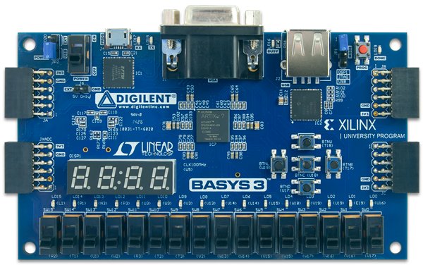
In the center of this board is an Integrated Circuit (IC) device called a Field Programmable Gate Array or FPGA (this is the square device labeled ARTIX-7). This FPGA device is the heart of the board and contains the programmable digital logic that you will use in most of your lab exercises. An FPGA device is a programmable digital circuit that can be configured to perform different functions based on the user’s digital design. Other major components of the Basys 3 board that you will use this semester include:
- 4-digit seven-segment display
- 16 switches
- 16 LEDs
- 5 push buttons
- a USB/UART interface
- a VGA display interface More details about this board can be found by referring to the Basys3 Reference Manual.
You will be creating digital circuit designs during the semester and placing these circuits onto the FPGA device. The circuit that is configured onto the FPGA is defined in a file called a bitstream. These files are created by software from the manufacturer of the FPGA. You will be creating your own circuit bitstreams throughout the semester (but not in this lab). The following page contains a video with an overview of this Basys3 board: Overview of the Basys3 Board. To use your board, the jumpers need to be set properly. Check to make sure the blue jumpers are set as shown in the Basys3 jumpers tutorial. If they are not set properly, correct them.
What is the proper jumper setting of Jumper JP1?
What is the proper jumper setting of Jumper JP2?
Connect the Basys3 board to your host computer in the digital lab and turn on its power using the switch in the top left corner of the board. When you first turn the board on, the FPGA device will be programmed with a configuration file for a digital circuit that is saved on the board’s flash memory. Once the FPGA has been configured (as indicated by the green DONE LED in the top right corner of the board), the circuit is operational.
During the course of the semester you will be creating digital designs that will be configured onto the FPGA of the Basys3 board.
Sophisticated software will be used to convert your digital design into a configuration bitfile file that can be configured onto the board (you will be introduced to these tools in the next laboratory).
There are a number of ways to configure the Basys3 board with a bitfile.
The preferred way to do this in the digital lab is to execute the ../resources/openocd.py Python script within your classroom repository.
Configure your Basys3 board with the basys3_explore.bit bitfile that is provided to you by the startercode in your classroom repository by executing the following command:
python3 ../resources/openocd.py basys3_explore.bit
Additional approaches for downloading the bitfile on other platforms is found at the following tutorial.
Exercise #3 - Interacting with the Basys3 Board
In this next exercise, you will interact with the bitfile you configured in the previous exercise to learn more about the Basys3 board. Several activities are associated with this exercise to help you become familiar with the Basys3 board and its components.
Switches and LEDs
A primary user input to the FPGA circuit on the Basys3 board are the toggle switches. The board contains 16 switches (named SW15-SW0) in a row on the bottom of the board with SW0 being the right-most switch and SW15 being the left-most switch. The switches are labelled on the silkscreen of the circuit board (the silkscreen is the white text on the board that labels the components on the board). Each switch can be placed in the Up (ON or binary 1) or Down (OFF or binary 0) position. You will be using the switches in your future laboratory assignments and for a number of the activities in this exercise in this lab.
The Basys3 board also contains 16 light-emitting diodes (LEDs) located directly above each switch. These LEDs are labelled LD15-LD0 with LD0 being the right-most LED and LD15 being the left-most LED. The FPGA circuit configured on the FPGA can set the value of each of these LEDs. The LEDs can provide output functionality for user circuits.
The example bitfile is configured to perform eight different logic functions based on the values of the first four switches (SW3-SW0). The outputs of these eight logic functions are displayed on the first eight LEDs (LD7-LD0) on the Basys3 board. For example, the logic function for the first LED (LED0) is the ‘AND’ function and will only be turned on when all four switches are in the ‘ON’ or up position (i.e., LED[0] = SW[3] & SW[2] & SW[1] & SW[0]).
For this activity, you need to determine the logic function of the other seven LEDs.
Match each LED (LED0-LED7) to the corresponding logic function
What FPGA pin is LED0 connected to? (refer to the Basys3 reference manual). The pin number is one or more letters followed by a number (i.e., A0)
Push Buttons and Seven Segment Display
Another form of input to the FPGA circuit on the Basys3 board are the five push buttons. The five buttons are organized in a cross pattern on the right side of the board. The buttons are named based on their position on the cross pattern. “BTNC” is the center button, “BTNL” is the left button, “BTNR” is the right button, “BTNU” is the up button, and “BTND” is the down button. The buttons will provide a logic ‘1’ input to the FPGA while the button is pressed and a logic ‘0’ when the button is released.
The Basys3 board also has a four-digit “seven-segment display”. Each digit of the seven-segment display can display a hexadecimal number from 0 to F. With four digits, a four-digit seven-segment display can display a 16-bit hexadecimal number. You will design a seven segment display controller in a future lab.
Press the right button on the Basys3 board (BTNR) and indicate what value is displayed on the seven segment display
Clocking and Counters
Digital circuits operate with a clock signal that synchronizes the operation of the circuit. The clock is used to increment counters, load internal registers, and sequence state machines. You will be designing a number of circuits over the semester that use the clock signal. The Basys3 board has a clock chip that generates a periodic clock signal for the FPGA (see the “Oscillators/Clocks” section of the Basys3 Reference Manual).
What is the frequency of the clock signal provided by the Basys3 board?
What FPGA pin is the clock signal connected to?
A “free running” 32-bit counter has been implemented in this example circuit. This counter increments its value by 1 every the clock signal transitions from low to high. You can view the value of this free running counter on the seven segment display by pressing the “Down” button (BTND) on the Basys3 board. When BTND is pressed, the seven segment display will display the lower 16-bits of the counter value when switch 0 is in the down position and the upper 16-bits of the counter when the switch is in the up position.
How long will it take for this 32-bit free running counter to overflow?
Universal Asynchronous Receiver/Transmitter (UART)
The Basys3 board has a Universal Asynchronous Receiver/Transmitter (UART) interface that can be used to communicate between the FPGA and the host computer through the USB port. You will be designing an asynchronous transmitter and receiver in future labs.
To communicate with the Basys3 board you will need to run an application program named ‘PuTTY’ on your host computer. Follow the instructions at the following PuTTY Tutorial to setup PuTTY for this activity.
The example bitfile is configured to send 8-bit ASCII characters from your Basys3 board to the host computer. To transfer an 8-bit ASCII character from the Basys3 board to the host computer, set the 8-bit ASCII value on switches SW15-SW8 (the hex value of these switches will be displayed on the left two digits of the seven segment display). Once the switches contain the desired 8-bit ASCII value, press the “Center” button (BTNC) on the Basys3 board to initiate the transfer. If PuTTY is set up properly, you will see the 8-bit ASCII character on the PuTTY terminal.
For this activity, send the characters of your ‘netid’ to the PuTTY terminal so that only your netid is displayed on the terminal. Use lowercase characters for the letters. You can find the ASCII values of these characters at the following ASCII Table. The following control commands can be sent over serial device from your board to control the PuTTY terminal:
- 8’h08 - Back Space (move curser back one character)
- 8’h0A - Move cursor down (Line Feed)
- 8’h0C - Clear screen
- 8’h0D - Carriage Return
- 8’h7F - Delete (move curser back one and delete)
When you have successfully sent your netid to the PuTTY terminal, take a picture of the PuTTY terminal with your netid displayed (the following tutorial describes how to take screenshots on the digital lab computers).
Rename the .png file to netid.png and add it to your lab01 directory.
Note that screenshots have guidelines that must be followed to avoid penalty.
Review the guidelines at the end of the previously linked tutorial.
Include the file netid.png in the ‘lab01’ directory of your repository.
In addition to a transmitter that sends data from the Basys3 board to the host computer, the Basys3 board is also configured with a receiver that can receive data from the host computer. With the PuTTY application in focus, type a character on the keyboard of the host computer and see the value of the character displayed on the right two digits of the seven segment display. Press a few characters within the PuTTY terminal and watch the seven segment display update with the ASCII value of the character.
What is the ASCII value you receive if a Ctrl-J is pressed in PuTTY?
VGA Display
The Basys3 board has a VGA display interface and that can be used to display images on a VGA monitor. Digital circuits can be created to generate the VGA timing signals and pixel color signals to display custom images on the monitor. You will create a VGA display controller in a future lab. The example bitfile is configured to display a 640x480 pixel image on the VGA display.
Connect your Basys3 board to the VGA display cable that is provided at each station in the digital lab. Change the display input on the monitor to select the VGA input rather than the display port input used for your computer. The Selecting the Display Video Input describes how to do this.
If your Basys3 board is properly connected to the VGA display and the example bitstream is configured on the FPGA, you should see a blank screen with a color based on the value of the switches SW15-SW4. The VGA interface supports the generation of a 12-bit color signal. Four bits are allocated for “Red” (where 1111 is the maximum intensity of red and 0000 is no red), four bits are allocated for “Green”, and four bits are allocated for “Blue”. A custom color is created by mixing different intensity values for Red, Green, and Blue. You could set the color of the screen by changing the values of the switches SW11-SW0. The switches are defined as follows:
- SW11-SW8: Red
- SW7-SW4: Green
- SW3-SW0: Blue
Experiment with different switch settings to create different colors on the VGA display.
Press the left button (BTNL) on the Basys3 board to display a color bar pattern with eight vertical color bars displayed on the top half of the display. Determine the binary value of each of these eight color bars. For example, the leftmost color bar is “Black” with the color value of 0000 0000 0000. You can use the switches to change the color of the bottom half of the screen to match the color of the corresponding column.
What are the values of the eight color bars? (answer as a 12-bit binary number)
The VGA display controller configured on the FPGA will generate a new frame multiple times a second. The number of frames that have been generated by the VGA core can be determined by pressing the up button (BTNU) on the Basys3 board. Determine the approximate number of frames per second generated by the VGA core by pressing the BTNU button at two different time intervals.
Determine the number of frames per second that the VGA display is running at.
Pass-Off
In order for you to receive any credit for the “passoff” portion of the laboratory assignment, you must successfully complete the full pass-off process. The pass-off process is involved and requires multiple steps. It is essential that you understand and follow the instructions carefully - if you do not understand or follow these instructions carefully you may not receive any credit for the passoff portion of the lab. A passoff tutorial has been created to help you understand the passoff process. Follow this tutorial carefully and complete each of the steps in this process.
- Required Files
aboutme.txtnetid.pngMakefile(this file is required for all assignments).gitignore(this file is required for all assignments)
- Required Makefile ‘rules’
about(generates fileaboutme.txt)reverse(generates filereverse.txt)upper(generates fileupper.txt)lineno(generates filelineno.txt)bottom(generates filebottom.txt)clean(this rule is required for all assignments)
After completing the lab, you are required to answer the following two questions in your lab report. These questions help us gather feedback for the complexity and difficulties of the lab, so we can improve the lab for future semester.
How many hours did you work on the lab?
Provide any suggestions for improving this lab in the future
Congratulations! You have completed your first laboratory assignment for ECEN 320. You should be well-prepared to complete the future laboratory assignments in this class.