Table of Contents
- Learning Outcomes
- Preliminary
- Top-Level Design
- Exercises
The purpose of this laboratory is to create a character generator circuit for displaying ASCII text characters on the VGA display. You will also create a simple circuit that writes characters to the screen using the switches and buttons.
The average time to complete this lab last year was 8 hours; however, changes have been made to shorten the lab time this year, and we will review the preliminary material in class ahead of time.
Learning Outcomes
- Understand how to use internal BRAM memories
- Draw characters from a font ROM onto the screen
Preliminary
Character Display Organization
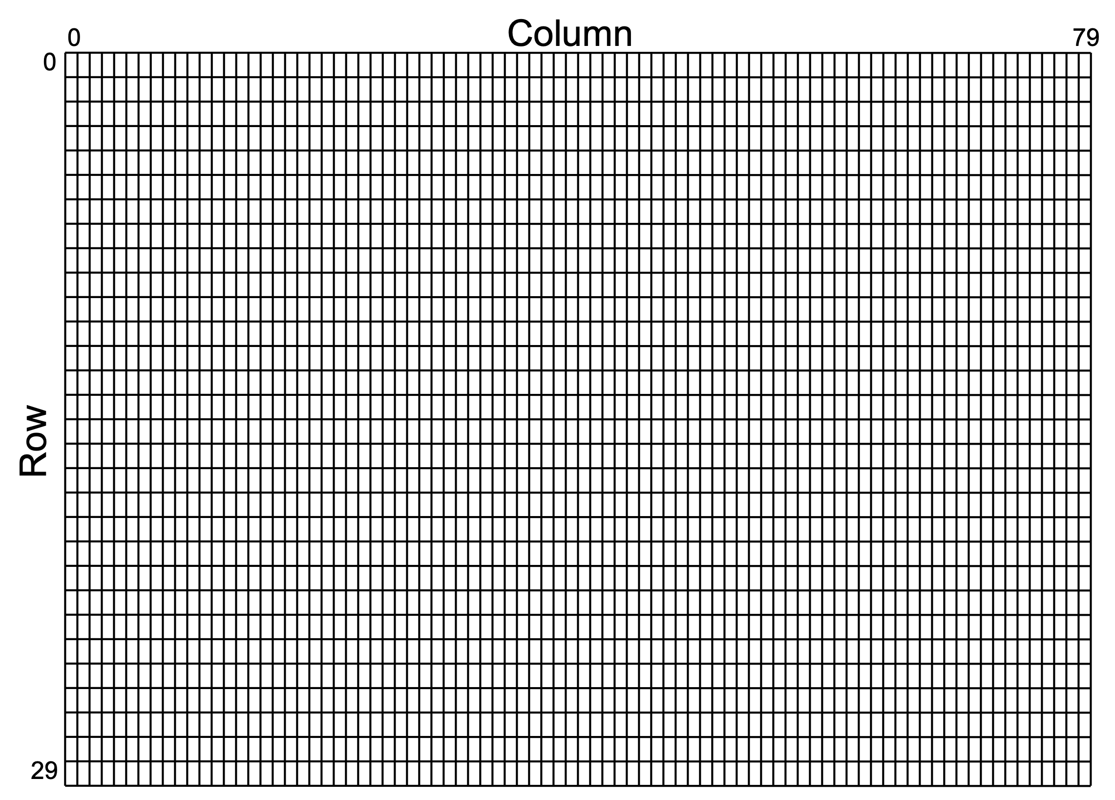
Displaying text is an important function of a video controller. Dedicated circuits are often used to facilitate the display of text characters on a screen. To display text on our VGA display, we will organize the 640x480 display area into larger “tiles” where each tile represents a character location. In this lab, the size of each character is 8 pixels wide and 16 pixels high. Mapped onto a 640x480 display, this font will display 80 text characters in each line (i.e., 640 pixels for each row divided by 8 columns per character) and 30 lines (i.e., 480 lines divided by 16 pixels per character, 480 / 16). The layout of the 80 x 30 character screen is shown below.
When drawing text characters on the screen, we will refer to several coordinate systems.
The first coordinate system is the display coordinate system, used for locating individual pixels on the display (i.e., 640x480).
The top left pixel of the display is labeled (0,0), and the lower right pixel of the display is (639,479).
The pixel_x and pixel_y outputs from the VGA timing controller reference this display coordinate system.
The character coordinate system is used to specify the location of characters on the screen (i.e., the 80x30 character layout shown above). The top left character position is (0,0), and the lower right character is (79,29). Every pixel in the display is mapped to one of these characters. To convert the x coordinate of a pixel into its corresponding character column is done by dividing the x pixel value by 8 without rounding. To convert the y coordinate of a pixel into the corresponding character row is done by dividing the y pixel value by 16 (again without rounding). For example, the pixel (x=35, y=41) in the display coordinate system will map to the character located at character position (4, 2) (i.e., 35/8, 41/16), which contains the ‘T’ in the figure above.
This division can easily be done in digital hardware by taking the top seven bits of pixel_x for the x-character location, and taking the top five bits of pixel_y for the y-character location.
The following SystemVerilog code demonstrates how to generate the character positions from the pixel positions:
assign char_x_pos = pixel_x[9:3];
assign char_y_pos = pixel_y[8:4];
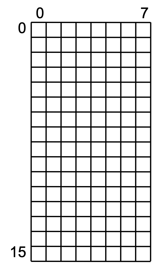
There is also a sub-character coordinate system for pixels within an individual character. As described above, each character is 8 pixels wide and 16 pixels high. The position of the top left pixel of a character is (0,0), and the lower right pixel of a character is (7,15) as shown in the figure below.
Every pixel in the display coordinate system maps to a specific character in the character coordinate system and to a pixel within the sub-character coordinate system.
The x and y locations in the sub-character coordinate system can be found by performing a modulo 8 and modulo 16 operation on the pixel_x and pixel_y values, respectively.
Since these are powers of 2, this can be done easily in hardware by just taking the lower bits of the pixel_x and pixel_y values:
assign char_x_pixel = pixel_x[2:0];
assign char_y_pixel = pixel_y[3:0];
Answer the following questions to demonstrate your understanding of the organization of the characters on the display:
How many characters can be displayed on the 640 x 480 display using this font?
What is the character coordinate associated with the pixel at location (279, 173)
What is the sub-character coordinate associated with the pixel at location (279, 173) (i.e., what position is this pixel within a 8x16 character)?
Font ROM
The appearance of the characters on the screen is determined by a font ROM.
The font ROM is a read-only memory that stores the pixel pattern for each character in the character set.
This is provided to you as char_gen/font_rom.sv.
The font ROM stores one bit for each of the 8x16 pixels for each character, for a total of 128 bits per character.
A ‘1’ indicates the pixel should be displayed in the foreground (i.e., white for white text), while a ‘0’ indicates the pixel is in the background.
The font ROM is organized as a 1-D array of 8-bit words, where each word corresponds to one row of pixels for a character.
The text below demonstrates the contents of the font ROM for the upper-case character ‘A’:
   8'b00000000, // 0
   8'b00000000, // 1
   8'b00010000, // 2    *
   8'b00111000, // 3   ***
   8'b01101100, // 4  ** **
   8'b11000110, // 5 **   **
   8'b11000110, // 6 **   **
   8'b11111110, // 7 *******
   8'b11000110, // 8 **   **
   8'b11000110, // 9 **   **
   8'b11000110, // a **   **
   8'b11000110, // b **   **
   8'b00000000, // c
   8'b00000000, // d
   8'b00000000, // e
   8'b00000000, // f
The font ROM for the character ‘A’ shown above will create the character shown below:
The font_rom.sv contains pixel patterns for all 128 characters in the 7-bit ASCII character set, including upper and lower case letters, numbers, punctuation, and special characters.
Since each character takes 16 rows in the ROM, the entire character set takes 128 characters x 16 rows/character = 2048 rows in the ROM.
In essence, we are mapping a 2-D array of data (128 characters and 16 rows/character) into a 1-D ROM.
Since these are powers of two, we can easily generate the ROM address for a given character and row by taking the character value (7 bits) as the upper bits of the address and the row number (4 bits) as the lower bits of the address.
This ROM fits into the size of a single BRAM and will be mapped to one of the BRAMs on your FPGA board. The font ROM is a synchronous memory, meaning it requires one clock cycle to access the memory contents.
Answer the following questions after reviewing the char_gen/font_rom.sv file:
How wide, in bits, is each word of this ROM?
How many bits are required to define a single character in this ROM?
What is the total size, in bits, of this ROM?
What is the value of the word at address 0x32a in this ROM?
What character is associated with address 0x32a in this ROM?
What is the first address in the font ROM that stores the contents for the character ‘A’?
Assume that pixel_x=279 and pixel_y=170 and you are trying to display the character ‘A’. What index will you read from in the font rom?
Assuming the same situation described in the previous question, what is the corresponding pixel value for the character ‘A’ at the given location?
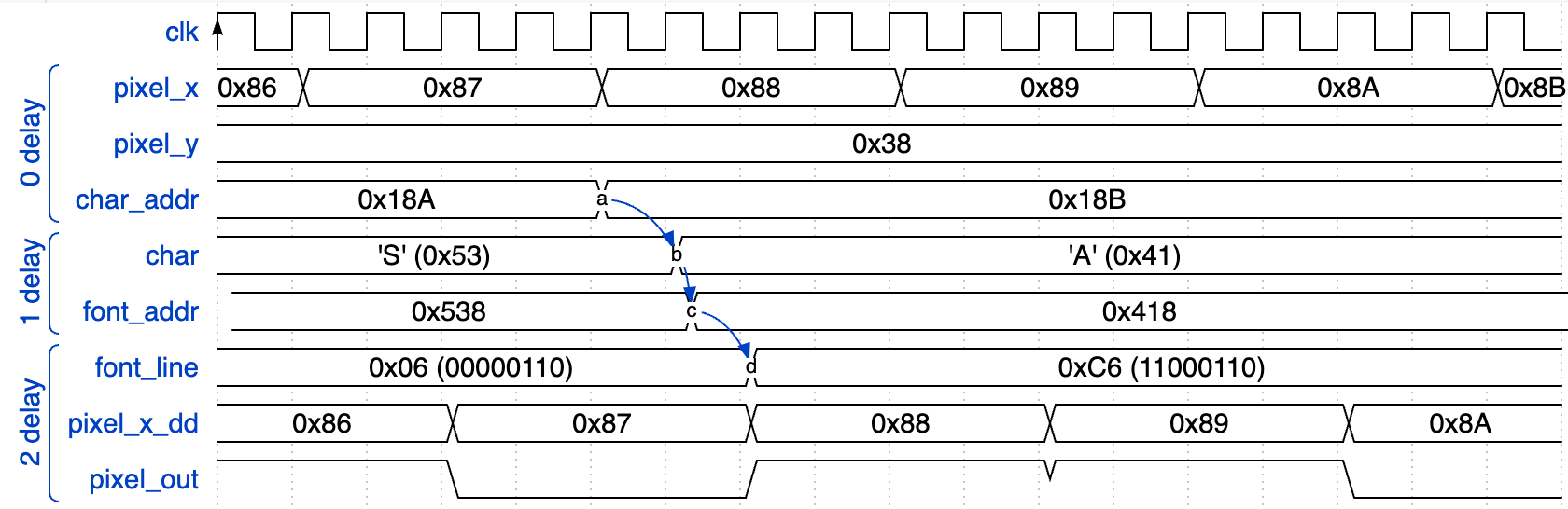
Refer to the timing diagram below and answer the following questions. For each answer, provide your response as an 8-bit SystemVerilog value (i.e., 8’b00000000).
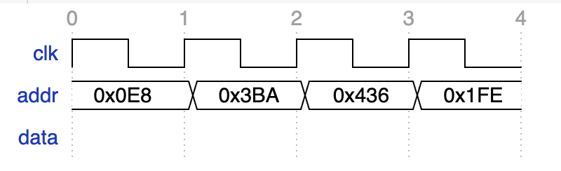
What is the value of the ‘data’ output between clocks 1 and 2 (i.e., 1.5)?
What is the value of the ‘data’ output between clocks 2 and 3?
What is the value of the ‘data’ output between clocks 3 and 4?
Top-Level Design
The goal of this lab is to maintain a memory (called the character memory) of which character should be displayed at each position on the screen, and to display them on the screen by looking up the appropriate pixel patterns from the font ROM. It’s not very interesting to just have a static display; we also want to be able to change which characters are displayed on the screen. Our top-level design will allow the user to write new characters to the memory using two methods:
- Sending a character over UART.
- Setting the switches to a character value and pressing a button to write that character to the screen.
In both cases, you will maintain an invisible cursor on the screen that indicates where the next character will be written. This will increment left-to-right and top-to-bottom as new characters are received.
To implement this system, you will create the following top-level design that integrates several of the components you have designed in previous labs, including the VGA timing controller, the UART receiver, and the seven segment display controller.
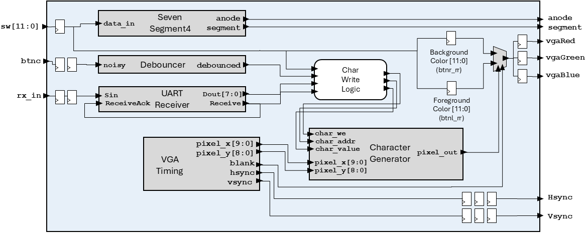
Note: The above diagram does not show every element of the design, certain items are omitted for clarity (e.g., clocks, resets, and logic for updating the foreground and background colors).
Some notable items in the design include:
- The VGA timing controller constantly iterates through all pixel locations on the screen, outputting the current pixel coordinates (
pixel_xandpixel_y) and synchronization signals (h_syncandv_sync). The main challenge of this lab, is to determine what color to output for each (x, y) pixel, foreground (i.e., the text color) or background. - The Character Generator module, which is discussed in more detail later, internally contains a memory of which character to display at each position on the screen, and an instance of the font ROM to determine how to draw each character. The character generator takes the current pixel coordinates as input and outputs whether the pixel should be foreground or background based on the character memory and font ROM.
- Multiplexing logic uses the
pixel_outsignal from the character generator to determine whether to output the foreground or background color for each pixel, or to output black for the blanking intervals. The color is fed through registers before being output to the VGA ports to eliminate any output glitching. Theh_syncandv_syncsignals are fed through three registers to balance the latency of the character generator module. - The Character Generator also has a write port, that allows the top-level design to change which character is stored at each position on the screen. The Char Write Logic, takes outputs from the UART receiver and the switches and
btncto determine when to write a new character to the character memory. Whenever a new character is received from the UART or thebtncis pressed, the char write logic will write a new character to the character memory at the current cursor location, and then update the cursor location to the next position on the screen. - When
btnlis pressed, the foreground color is updated to the value of the switches, and whenbtnris pressed, the background color is updated to the value of the switches. - For convenience, the 4-digit seven segment display is used to show the decimal value of the switches.
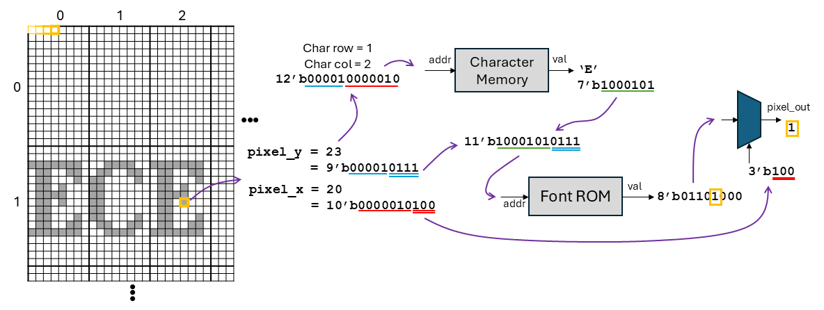
The Character Generator
This module:
- Stores which character to display at each position on the screen in a memory called the character memory, and allows writing to this memory to change the characters that are displayed on the screen.
- Can be provided with a specific pixel location (
pixel_xandpixel_y) and will determine whether the pixel at that location should be on (i.e., foreground) or off (i.e., background) based on the character memory and the font ROM (it has an instance of the font ROM within it), and outputs a1or0on thepixel_outport.
The following diagram illustrates how the character generator uses the character memory and the font ROM to determine whether a given pixel should be foreground or background. Review these slides for an explanation of this example.
Exercises
Make sure to merge in any changes from the startercode before starting the lab.
The following are the exercises for this lab:
- Exercise #1: Character Generator: Create the character generator module.
- Exercise #2: Character Generator Simulation: Simulate the character generator module to verify that it is working correctly.
- Exercise #3: Character Generator Testbench: Verify the character generator module is working correctly with the provided testbench.
- Exercise #4: Top-Level Design: Create the top-level design described above.
- Exercise #5: Top-Level Simulation: Simulate your top-level design to verify it is working correctly.
- Exercise #6: FPGA Implementation. Create a bitstream for your design.
- Exercise #7: Download and Test. Download your design to the FPGA and verify it is working correctly by writing characters to the screen using the buttons and switches, and by sending characters over UART.
Exercise #1: Character Generator
Begin this exercise by creating a new SystemVerilog file named char_gen/char_gen.sv with the following ports:
| Parameter | Default | Function |
|---|---|---|
| FILENAME | ”” | Specifies the filename of the initial contents of the memory |
| Module Name: char_gen | |||
|---|---|---|---|
| Port Name | Direction | Width | Function |
| clk | Input | 1 | 100MHz System Clock |
| char_we | Input | 1 | Character write enable |
| char_addr | Input | 12 | The write address of the character memory |
| char_value | Input | 7 | The 7-bit value to pad and write into the character memory |
| pixel_x | Input | 10 | The column address of the current pixel |
| pixel_y | Input | 9 | The row address of the current pixel |
| pixel_out | Output | 1 | The value of the character output pixel |
Note: The flip-flops in this module do not require resets, so this module does not contain a reset signal.
Character Memory
First write the RTL for the character memory. This memory stores which character to display at each of the 80x30 positions on the screen. The memory will have two synchronous *ports (operating on the rising edge of the clock signal):
- A write port for occasionally changing which character is stored at a given position.
- A read port for retrieving the character stored at a given position (this will be used constantly to drive the VGA display with the appropriate character data).
The diagram above shows this memory as a separate module, with write (wr_*) and read (rd_*) ports, and a clk input. You might think we should instance a memory block and wire up to these ports. However, instancing an FPGA memory block directly from our code is somewhat complex and unnecessary. In the previous labs you have written behavioral always_ blocks and the synthesis tools has automatically mapped these to FPGA LUTs and flip-flops.
Similarly, we will describe a memory behaviorally using always_ blocks, and the synthesis tools will automatically map this to one of the FPGA BRAMs.
As such, the code we write will look a bit different than the diagram above, but the resulting circuit will match the diagram.
You do not need to create a separate module for the character memory, we will describe the character memory behaviorally within the char_gen module, as described in the following steps.
-
Begin your memory by defining an array of logic values of size 4096 x 8 bits.
logic [7:0] mem_data[0:4095];This ROM needs to store the 7-bit ASCII value for each character in the 80x30 character grid. However, since these sizes are not powers of two, we will use a larger memory that is sized with powers of two to simplify our design. We will use an 8-bit memory, with 4096 entries. Like the font ROM, this memory will be storing a 2-D array of data in a 1-D memory, so we will split the address into two parts:
- The upper five address bits (
char_mem_addr[11:7]) will choose the character row (0 through 29) - The lower seven address bits (
char_mem_addr[6:0]) will choose the character column (0 through 79) - There is some wasted memory, but it allows for a simpler design and more efficient address decoding.
Answer the following questions to demonstrate your understanding of the character memory.
How many bits are stored in the character memory?
What address of the character memory holds the value for the character located on the character display at col,row = (65,17)?
What are the character coordinates of the character stored at address 0xB8F in the character memory?
- The upper five address bits (
-
Create synchronous logic to write values into the character memory (called the write port).
The write port is used to change which character is stored at each location, and is controlled using the address (
char_addr), the value to write (char_value), and the write enable signal (char_we).The write port logic is described with an
always_ffblock that updates the value of a given index in themem_dataarray:mem_data[char_addr] <= ...;When you write to
mem_data, pad thechar_valuewith a1'b0in the most significant bit since thechar_valueis 7 bits but themem_datais 8 bits. -
Create a synchronous read port for the character memory.
The read port is used by the character generator circuit to determine which character is supposed to be displayed at a particular
pixel_xandpixel_ylocation. The read port logic is also described with analways_ffblock that reads the value from themem_dataarray, and stores it in an internal signal calledchar_read_value:char_read_value <= mem_data[char_read_addr];Note: There is no read enable signal for the read port; the memory is always being read.
You will need to use combinational logic to generate the 12-bit
char_read_addrsignal, based on thepixel_xandpixel_yinput ports. Look at the example in the preliminary section to see how this is done. -
Initialize the memory contents from a file (if specified).
The character memory array can be initialized with an initial set of characters through an initialization file. Add an
initialblock to your character generator module to initialize the contents of the memory if theFILENAMEparameter is set:initial begin if (FILENAME != "") $readmemh(FILENAME, mem_data, 0); end
Font ROM
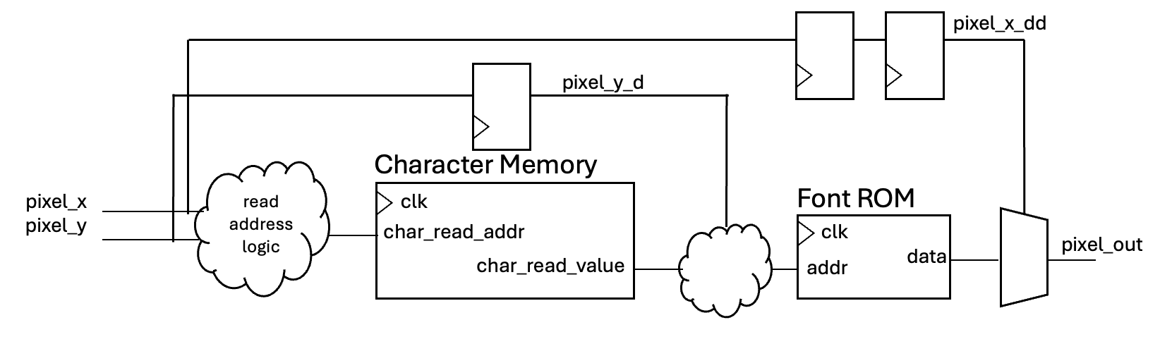
- Instance the font ROM in your character generator module.
- Connect up the address input of the font ROM appropriately, based on the character value output from the character memory and the row within the character determined by the
pixel_yinput. Look at the example in the preliminary section to see how this is done. - Note that due to the 1-cycle latency of the character memory, the
char_read_valueis delayed by one clock cycle from thepixel_ysignal. Feed thepixel_ysignal through a one-cycle pipeline register to create a delayed version ofpixel_y(call thispixel_y_r). - Create an 8-bit signal,
rom_data, connected to the output of the font ROM.
Pixel Out Multiplexer
Create multiplexing logic to select the appropriate pixel from the font ROM output to drive the pixel_out signal.
See the example in the preliminary section to see how the pixel selection is done.
Since the font ROM adds a cycle of latency, the output is now two cycles behind the pixel_x signal.
To compensate for this delay, pass the pixel_x signal through two registers before using it in the multiplexing logic.
Include the file char_gen/char_gen.sv in your repository.
Exercise #2: Character Generator Simulation
After creating your module, create a Tcl simulation script for your module. Your tcl file should include the following:
- Run the simulation for 100ns without setting any values
- Create a 100 MHz oscillating clock and run for a few clock cycles
- Perform a character write to location 0x000 with the value 0x41 (ASCII ‘A’) and run for a few clock cycles
- Set the
pixel_yvalue to ‘2’ and setpixel_xto values 0 through 7 to see the character ‘A’ displayed for row 2 - Do the same thing as above but for
pixel_y=3
Note that when you simulate your module, the memory will not be initialized with any values. This is okay; you will be loading a character into the memory during the simulation. Take a screenshot of the waveform.
Include the file char_gen/sim.tcl in your repository.
Include the file char_gen/sim.png in your repository.
Exercise #3: Character Generator Testbench
After simulating your module and verifying it operates with the Tcl script, you will need to test your receiver with the testbench. You may want to begin by testing the decoder interactively in GUI mode with this testbench to resolve syntax and behavioral problems in your design.
Make sure that the testbench simulates without any errors before proceeding.
Exercise #4: Top-Level Design
Create a new file named char_gen_top/char_gen_top.sv and include the following ports:
| Parameter | Default | Function |
|---|---|---|
| FILENAME | ”” | Specifies the filename of the initial contents of character memory |
| CLK_FREQUENCY | 100_000_000 | Specifies the frequency of the clock in Hz |
| BAUD_RATE | 19_200 | Determines the baud rate of the receiver |
| WAIT_TIME_US | 5_000 | Determines the wait time, in micro seconds, for the debounce circuit |
| REFRESH_RATE | 200 | Specifies the display refresh rate in Hz |
| Module Name: char_gen_top | |||
|---|---|---|---|
| Port Name | Direction | Width | Function |
| clk | Input | 1 | 100MHz System Clock |
| btnd | Input | 1 | Reset |
| btnc | Input | 1 | Write character |
| btnl | Input | 1 | Set background color |
| btnr | Input | 1 | Set foreground color |
| rx_in | Input | 1 | UART Receiver Input |
| sw | Input | 12 | Determines character to write or color to display |
| Hsync | Output | 1 | Horizontal synchronization signal |
| Vsync | Output | 1 | Vertical synchronization signal |
| vgaRed | Output | 4 | Red color signal |
| vgaGreen | Output | 4 | Green color signal |
| vgaBlue | Output | 4 | Blue color signal |
| anode | Output | 4 | Anode signals for each of the four display digits |
| segment | Output | 8 | Cathode signals for seven-segment display |
Review the top-level design diagram above and the descriptions of each component before starting this exercise. Implement the top-level design, and be sure to follow these specifications:
- The inputs (
btnd,btnc,btnl,btnr, andrx_in) should go through two flip-flop synchronizers before being used. The switches (sw) should go through one flip-flop synchronizer. - Use the
seven_segment4module to display the value of the switches. Attach the switches (lower 12) to the input to the display and only display the right three digits, with no decimal points. - Create two 12-bit registers for the foreground and background colors. On reset, the background color should be initialized to
12'h000(black) and the foreground color to12'hfff(white).Whenbtnlis pressed, set the background color to the value of the switches. Whenbtnris pressed, set the foreground color to the value of the switches. - Instance the VGA timing controller from the VGA display lab, and connect as shown in the diagram.
- Instance the
char_genfrom the previous exercise, and connect as shown in the diagram. For now, create internal signalschar_we,char_addr,char_value, andpixel_out, that will be assigned later. - Instance your UART receiver. Like the last lab, create an
acksignal that connectsReceivetoReceiveAckto immediately acknowledge any received UART data. - Instance your debouncer circuit for
btnc. - Review your instanced modules, make sure clock and reset are connected properly, and make sure any top-level parameters are passed correctly to the appropriate modules.
- Implement the Char Write Logic in the diagram to control when new characters are written to the character memory:
- Write a new character when
btncis pressed (a one-shot edge detector is needed here) or when a new character is received from the UART receiver (acksignal is high). - The character value to write should come from the switches when
btncis pressed, and should come from the UART receiver when a new character is received. - The address represents an invisible cursor on the screen that indicates where the next character will be written. Remember that the character memory address is 12 bits, where the upper five bits represent the character row and the lower seven bits represent the character column. Make sure to update the address appropriately after each character is written (i.e., increment left-to-right and top-to-bottom, and wrap around to the top after reaching the end of the screen). I.e,:
- If the character column is less than 79, increment the column by one.
- If the character column is 79 and the row is 29, set the column and row to 0.
- If the character column is 79, set the column to 0 and increment the row by one.
- Write a new character when
- Create the logic for the VGA color signals and timing signals as described below.
- When
blankis high, the RGB signals should be set to12'h000(black). - Otherwise, when
pixel_outis high, set the RGB signals to the foreground color, and when low, the background color. - Make sure the VGA signals are registered before being output to the VGA ports to eliminate any glitches.
- The
vgaRed,vgaGreen, andvgaBluesignals will be updated three cycles after the VGA timing controller outputs thepixel_xandpixel_ysignals (two cycles of latency from the character generator, and one additional cycle from the registers on the output). Make sure theHsyncandVsyncsignals are delayed by the same amount to keep them synchronized with the RGB signals.
- When
Include the file char_gen_top/char_gen_top.sv in your repository.
Exercise #5: Top-Level Simulation
Once you have created your top-level design, you will perform a short simulation to demonstrate the writing of character data is working properly.
Your top-level module should have a parameter named FILENAME that specifies the filename containing the initial contents of the character memory.
By default, this FILENAME is empty indicating that the memory should not be initialized with any values.
For this exercise, you will need to create a memory initialization file that initializes the character memory with Abraham Lincoln’s “Gettysburg Address”.
The text for this document is saved in the file gettysburg_address.txt.
A python script has been created for to convert this text file into a memory initialization file:
python3 gen_initial_chars.py gettysburg_address.txt gettysburg_address.mem
Simulate your top-level design with the following two parameters (note that you need the ../.. since the gettysburg_address.mem file is two directories up from the work directory where the simulation is run):
SIM_PARAMS = WAIT_TIME_US=50 FILENAME=../../gettysburg_address.mem
Create a TCL simulation file (sim.tcl) that does the following:
- Simulate loading the character
Sinto the character memory by pressingbtnc(make sure to give the button sufficient wait time to get through the debouncer) - Simulate loading the character
Ainto the character memory over the UART receiver (this is the same character sent in your previous lab - you can copy the tcl lines for performing this simulation).
Include the following signal in your simulation: clk, btnc, sw, rx_in, hsync, vsync, VGA signals, char_addr, char_we, and char_write_value.
Take a screenshot of the simulation showing the char_gen writes.
Include the file char_gen_top/sim.tcl in your repository.
Include the file char_gen_top/sim.png in your repository.
Exercise #6: Synthesis and Implementation
-
Create a
char_gen_top/basys3.xdcfile that contains pin location definitions for each of your I/O ports.Include the file
char_gen_top/basys3.xdcin your repository. -
For the synthesis and implementation step, you are required to create your own text message to display on the screen. Create a text file name
mymessage.txtthat includes inspirational, uplifting, or positive text that fills a good portion of the screen (i.e., the message uses the majority of the lines in the display). Create a Makefile rule namedmymessage.memthat generatesmymessage.memfile from your text message. Further, ignore the .mem file and clean the .mem file as part of the clean process. - Before running synthesis, you will need to use
SYNTH_PARAMSto set theFILENAMEappropriately.SYNTH_PARAMS = FILENAME=../../mymessage.mem -
Run synthesis and carefully review the synthesis log to make sure there are no warnings.
How many FDCE/FDRE/FDSE cells are used by the design?
How many total LUT resources are used by the design? (add up all the LUT* resources)
How many total Block RAMs are used by the design? (RAMB18E1 or RAMB36E1)
How many total IBUF and OBUF resources do you have in the design?
-
Run implementation.
-
Review the
timing.rptfile to answer the following questions.What is the Worst Negative Slack or ‘WNS’ of your design?
How many TNS total Endpoints are there in your design?
Open your implemented design in Vivado, and on the ‘Netlist’ tab to the left of the implementation view, expand the netlist to find the Font ROM component (something like: char_gen->fontRom->Leaf Cells->addr_reg_reg).
The cell type of the Font ROM is RAMB18E1.
Select this cell and take a screenshot of the memory resource.
Include the file char_gen_top/fpga.png in your repository.
Exercise #7: Download and Test
Once the bitstream has been generated, download your bitstream to the FPGA. Hook up your board to the VGA monitor and power it on to make sure the display is operating correctly. Test the ability to receive characters and display them on the screen by running ‘PuTTY’ as in the previous lab. Review the instructions for connecting your transmitter with PuTTY in the PuTTY tutorial. Set the baud rate to 19,200, 8 data bits, ODD parity, and 1 stop bit and connect to the appropriate COM port.
Final Pass-Off:
Refer to the passoff tutorial for the passoff process.
- See
required_filesin the passoff script. - Makefile rules that must work correctly and be free from errors and warnings:
Makefile:clean,mymessage.mem,gettysburg_address.memchar_gen/Makefile:sim_tbchar_gen_top/Makefile:synth,implement
Answer the final two questions in your laboratory report:
How many hours did you work on the lab?
Provide any suggestions for improving this lab in the future