A Xilinx Design Constraints file or .xdc file is needed to interface between your SystemVerilog modules and the Basys3 board.
An XDC file is required to generate a configuration bit file.
The XDC file performs the following important functions:
- Maps the inputs and outputs of your module to the physical pins on the FPGA and sets important properties for the pins, such as the voltage standard.
- Specifies important parameters for the synthesis and implementation tools
- Defines input clocks for synchronous designs. Each of these functions will be described below with examples.
Mapping Pins to Ports
On the Basys3 board, different pins on the FPGA are connected to different I/O on the board (eg. switches, buttons, and LEDs). These connections (red lines below) are part of how the PCB was designed and cannot be changed.
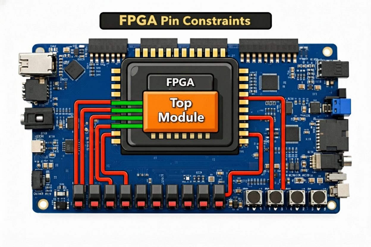
Vivado does not know which pins on the FPGA are connected to which I/O on the Basys3 board. Even though you may name your top-level port something like leds, it does not know which pins on the FPGA are connected to the LEDs on the board.
The Xilinx Design Constraints file or .xdc file is used to tell Vivado which pins on the FPGA should be connected to which top-level ports in your design (the green lines above).
Master XDC file
The creators of the Basys3 board have provided a XDC file that has a full mapping of all the pins on the FPGA to the I/O on the Basys3 board: https://github.com/byu-cpe/ecen320_student/blob/main/resources/basys3.xdc.
You will see many lines in the file like this:
set_property -dict { PACKAGE_PIN <PIN_NAME> IOSTANDARD LVCMOS33 } [get_ports { <PORT_NAME> }];
The PORT_NAME is the name of the top-level port in your SystemVerilog module that you want to connect to the pin, and the PIN_NAME is the name of the pin on the FPGA that you want to connect it to.
The following example command demonstrates assigning the led[0] port of a top-level Verilog design to pin W16 on the FPGA.
set_property -dict { PACKAGE_PIN W16 IOSTANDARD LVCMOS33 } [get_ports { led[0] }];
You will notice all of the lines in the Basys3 XDC file are commented out. To make your own XDC file for your design:
- Copy the provided
basys3.xdcfile to your design directory - Uncomment the lines that correspond to the pins your design uses.
- Modify the port names to match the top-level input and output ports of your design. Do this by changing the values inside the curly braces
{}of theget_ports { }portion of the command.In some labs, the top level port names will match what is already in the XDC file (sw[0]for example) and so you won’t have to change them. In other labs, the top level port names will not match what is already in the XDC file and you will have to change them in the XDC file.
Input Clock Specification
The input clock is a special signal that is used to synchronize the operation of the FPGA.
In addition to the conventional pin assignment for the clock, you need to identify this signal as a clock and specify the clock frequency.
The following example demonstrates how to specify the clock signal clk on pin W5 with a frequency of 100 MHz.
You will find these two lines near the top of the provided basys3.xdc file, commented out (you won’t need them until later labs):
set_property -dict { PACKAGE_PIN W5    IOSTANDARD LVCMOS33 } [get_ports { clk }];
create_clock -period 10.00 [get_ports { clk }];
Other Constraints
There are other constraints that you will find at the bottom of the provided basys3.xdc file that should be included in each of your designs:
## Configuration options, can be used for all designs
set_property CONFIG_VOLTAGE 3.3 [current_design]
set_property CFGBVS VCCO [current_design]

## SPI configuration mode options for QSPI boot, can be used for all designs
set_property BITSTREAM.GENERAL.COMPRESS TRUE [current_design]
set_property BITSTREAM.CONFIG.CONFIGRATE 33 [current_design]
set_property CONFIG_MODE SPIx4 [current_design]